Wave Soldering Comprehensive Guide: Principles, Process, & Optimization – S&M
- Introduction to Wave Soldering: The Basics of PCB Assembly
- The Science Behind Wave Soldering: Principles and Processes
- Key Components of a Wave Soldering Machine: Anatomy and Function
- The Wave Soldering Process: Step-by-Step Breakdown
- Types of Solder and Flux in Wave Soldering: Selection and Application
- Optimizing Wave Soldering Parameters: Achieving Peak Performance
- Common Wave Soldering Defects: Identification, Causes, and Troubleshooting
- Quality Control and Inspection in Wave Soldering: Ensuring Reliability
- Maintenance and Calibration of Wave Soldering Machines
- Wave Soldering vs. Reflow Soldering: A Comparative Analysis
- Environmental Considerations and Safety in Wave Soldering
- Emerging Trends and Future of Wave Soldering Technology
- Conclusion: The Enduring Role of Wave Soldering in Electronics Manufacturing
Introduction to Wave Soldering: The Basics of PCB Assembly
In the intricate world of electronics manufacturing, the assembly of Printed Circuit Boards (PCBs) is a cornerstone process that dictates the performance and reliability of countless devices. Among the various soldering techniques, wave soldering stands as a foundational method, particularly crucial for components with through-hole leads and mixed-technology assemblies. This comprehensive guide aims to demystify wave soldering, offering a detailed exploration of its principles, machinery, processes, and optimization strategies. From the fundamental science governing solder flow to advanced troubleshooting techniques, and from environmental stewardship to the cutting edge of technological innovation, we will provide engineers, technicians, students, and industry professionals with an exhaustive resource to master this indispensable PCB manufacturing process. By delving into the intricacies of wave soldering, readers will gain a foundational understanding essential for achieving peak performance, ensuring quality, and navigating the evolving landscape of electronics production.
The Science Behind Wave Soldering: Principles and Processes
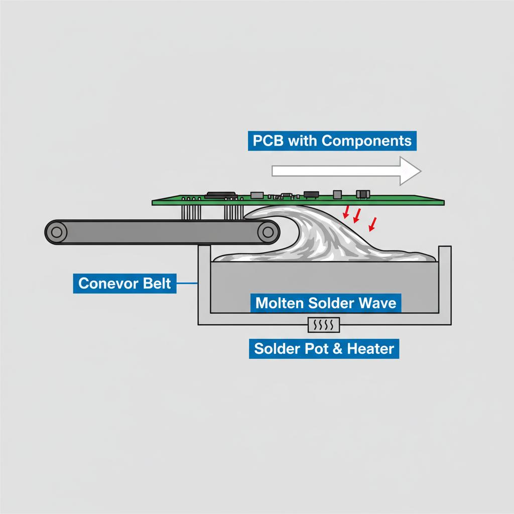
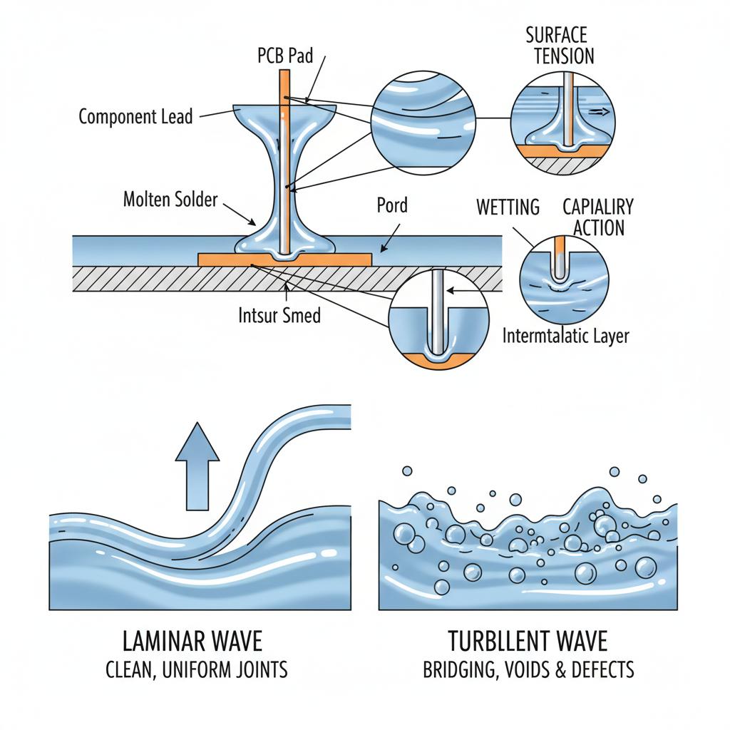
Wave soldering is a pivotal process in printed circuit board (PCB) assembly, known for its efficiency in soldering numerous connections at once. It involves the passing of PCBs over a wave of molten solder that ensures all of the electronic components are properly soldered onto the board. This method, which dates back to the mid-20th century, revolutionized electronics manufacturing by significantly reducing the time and complexity required for mass-produced electronics.
In the world of PCB assembly, wave soldering remains critical despite the emergence of alternative methods like reflow soldering. It excels in through-hole technology, delivering robust connections and is particularly favored for certain types of high-volume production where consistent quality and durability are paramount. For a more detailed comparison of these two methodologies, you can read our Wave Soldering Operation Guide.
Through this comprehensive guide, readers will dive into the intricate workings of wave soldering. We will explore the scientific principles that underpin the process, the anatomy of wave soldering machines, and the selection and application of different types of solder and flux. Further, we will provide a step-by-step breakdown of the wave soldering process and strategies for optimizing parameters to enhance performance. Additionally, our Comprehensive Guide To Preventing Solder Bridging In Wave Soldering offers valuable insights into enhancing soldering quality.
Readers will also gain insights into common defects associated with wave soldering, along with practical troubleshooting tips and quality control measures to ensure reliability. Additionally, we will compare wave soldering to reflow soldering to understand their differences and applications better, while considering environmental and safety considerations pertinent to wave soldering.
By the end of this guide, you will appreciate wave soldering’s enduring role in electronics manufacturing and be aware of emerging trends that may shape its future. As you read through this guide, keep in mind the practical guidance and technical insights aimed to enhance your understanding and proficiency in the art of wave soldering.
Key Components of a Wave Soldering Machine: Anatomy and Function
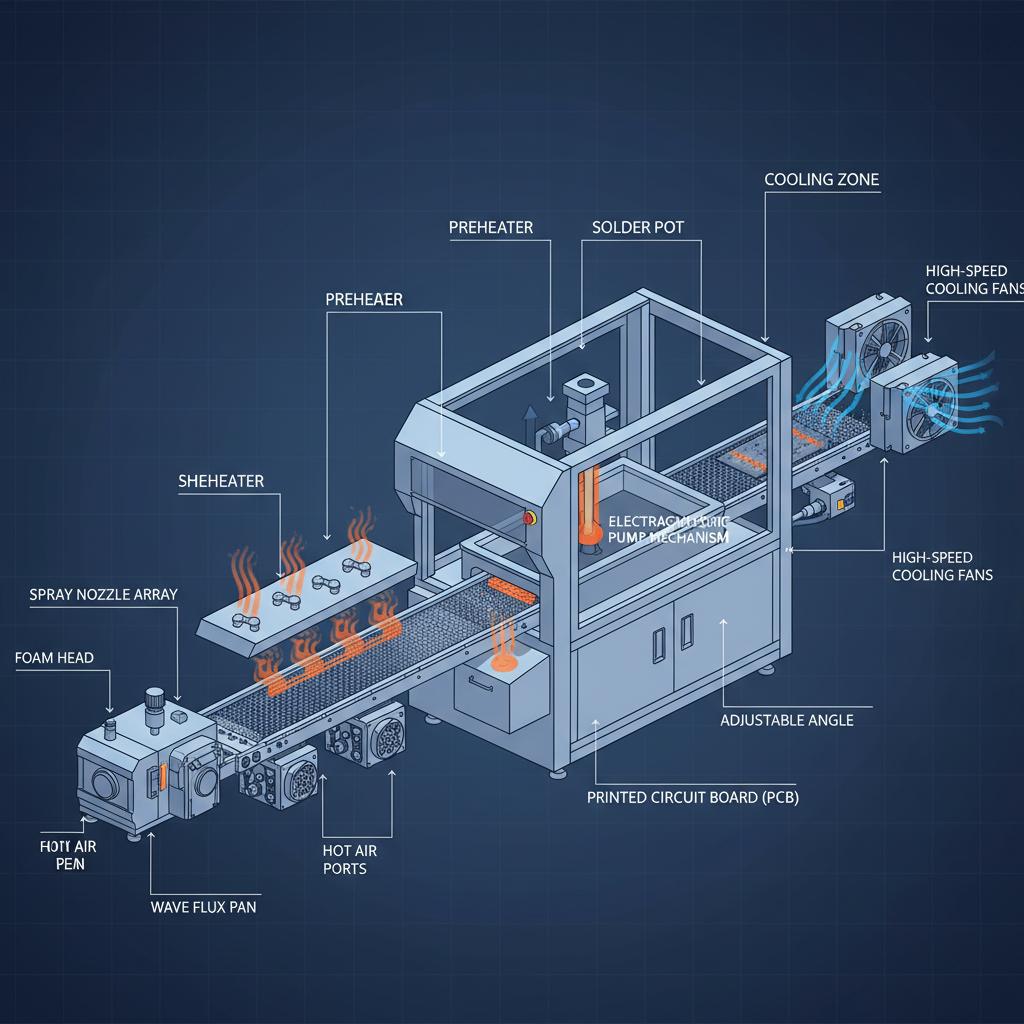
Wave soldering machines are intricate assemblies designed to efficiently solder electronic components onto PCBs using waves of molten solder. Understanding the anatomy and function of these machines’ key components is fundamental for optimizing performance and ensuring high-quality outcomes in PCB assembly.
Fluxer
The fluxer is a crucial component for ensuring a clean and receptive PCB surface prior to soldering. This subsystem can employ spray, foam, or wave mechanisms to apply flux evenly onto the PCB.
- Spray fluxer utilizes fine mist to cover larger areas uniformly, enhancing efficiency.
- Foam fluxer generates a foam barrier on the PCB to reduce oxidation risks.
- Wave fluxer provides targeted application with increased control.
The fluxer enhances solder wetting and helps prevent defects such as unwanted bridging and solder skips, making it indispensable for reliable solder adhesion.
For more insights on enhancing solder quality through flux applications, refer to our article on “Wave Soldering&Selective Fluxer: The Smart Combination for Enhanced Soldering Quality.”
Preheater
The preheater component serves to elevate the PCB temperature before it encounters the wave of molten solder, facilitating improved solder flow and adhesion. The preheater can harness infrared (IR), convection, or hot air technologies:
- IR preheating quickly radiates heat to the PCB surface.
- Convection preheating provides uniform heating across the board.
- Hot air preheaters allow for controlled and adjustable temperature.
Proper preheating minimizes the thermal shock experienced by components, reducing stress and enhancing solder joint integrity.
Solder Pot
The solder pot is the heart of the wave soldering machine, where solder is melted and maintained at an optimal temperature. Key features include:
- Pump mechanism facilitates the movement of molten solder, creating consistent waves.
- Heater ensures solder remains in its molten state for effective soldering.
- Dross removal handles accumulated impurities that can adversely affect solder quality.
Maintaining a consistent wave and ensuring purity in the solder through efficient dross removal are critical for high-quality, defect-free solder joints.
Fördersystem
The conveyor system controls the movement of PCBs through various stages of soldering:
- Angle and speed determine the rate at which boards are exposed to solder waves and influence solder penetration and exposure time.
Precision in conveyor operation ensures optimized contact time and proper heat dissipation, both crucial for quality soldering.
For more information on conveyor systems, refer to our “Automate On A Budget: The Essential Guide To Affordable PCB Conveyors.”
Kühlung Zone
The cooling zone solidifies the solder once the PCB exits the solder pot. Rapid and controlled cooling is essential:
- Cooling fan systems help in achieving desired cooling rates, which are crucial for forming strong solder bonds.
Efficient cooling prevents thermal stress and warping, which can compromise the integrity of solder joints.
Integrating visual aids like detailed diagrams can greatly enhance understanding of these components. Consider embedding product-specific case studies to illustrate these functionalities in practice, thereby turning theoretical insights into tangible benefits.
For deeper technical exploration, the differences between wave and reflow soldering, particularly concerning cooling rates and production volume cost comparisons, can aid in decision-making for electronics manufacturers, providing the practical guidance industry professionals need to optimize their soldering operations.
The Wave Soldering Process: Step-by-Step Breakdown
Wave soldering is a critical process in the assembly of printed circuit boards (PCBs), demanding precision and attention to detail to ensure quality and functionality. Understanding the step-by-step sequence is essential for achieving optimal results, particularly when comparing traditional soldering techniques like reflow soldering. Here’s a detailed look at each stage:
1. Flussmittel Anwendung
The first stage of the wave soldering process involves the application of flux to the PCB. Flux’s primary purpose is to clean the component leads and pads by removing oxides, thereby enhancing the wetting of solder. Critical parameters include flux type (rosin-based, water-soluble, etc.) and application method (spray or foam). The effect is immediate, ensuring surface readiness for soldering. For an in-depth understanding of flux application techniques, you may refer to our Wave Soldering Operation Guide.
2. Vorwärmen
Preheating the PCB is crucial to prepare for solder wave contact. This step serves multiple purposes: it activates the flux, minimizes thermal shock to components, and reduces the risk of warping. Temperature control is critical, with typical preheat settings ranging from 100°C to 150°C. Immediate effects include increased component and flux stability. For more insights into temperature control mechanisms that are also pivotal in reflow techniques, see our article on the Critical Role of Chillers in Reflow Oven Temperature Control.
3. Solder Wave Contact
As the PCB moves across the solder wave, the molten solder forms fillets on the component leads and pads. The wave height, contact time, and conveyor speed are critical parameters, determining solder coverage and joint formation. The immediate effect is the creation of strong, conductive connections between components and the PCB.
Types of Solder and Flux in Wave Soldering: Selection and Application
Wave soldering is a critical process in PCB assembly, requiring precision in both the choice of solder and flux. Understanding these materials is essential for optimizing performance and complying with industry standards.
Solder Alloys in Wave Soldering
Solder alloys are a cornerstone of the wave soldering process, with options that include both leaded and lead-free. Each type offers specific benefits and challenges, impacting the choice based on application requirements and regulatory guidelines.
Leaded Solder Alloys (Sn-Pb)
- Composition : Typically a mix of tin (Sn) and lead (Pb), commonly in a 63/37 ratio.
- Vorteile : Renowned for excellent wettability and thermal fatigue resistance.
- Anwendungen : Predominantly used in legacy electronics where RoHS compliance is not a constraint.
- Considerations : Due to environmental regulations, its application is restricted, pushing industries towards alternatives.
Lead-Free Solder Alloys (SAC Alloys)
- Composition : Commonly composed of tin (Sn), silver (Ag), and copper (Cu).
- Vorteile : Better thermal conductivity and mechanical strength, making them suitable for modern electronics.
- Anwendungen : Preferred in consumer electronics due to RoHS compliance. For insights on reflow techniques used with lead-free solders, refer to A Comprehensive Guide To The SMT Reflow Oven Process.
- Considerations : Generally higher melting points compared to leaded alloys, requiring adjustments in process parameters.
Flux Types in Wave Soldering
Flux plays a pivotal role in ensuring effective soldering by cleaning and preventing oxidation. Understanding the types and their properties aids in selecting the right flux for specific tasks.
In-Depth Analysis
1. Rosin-Based Flux
- Composition : Derived from natural resins mixed with activators.
- Vorteile : Provides excellent cleaning action and residue that can be accounted for in post-soldering operations.
- Anwendungen : Frequently used in high-reliability aerospace and military applications.
Optimizing Wave Soldering Parameters: Achieving Peak Performance
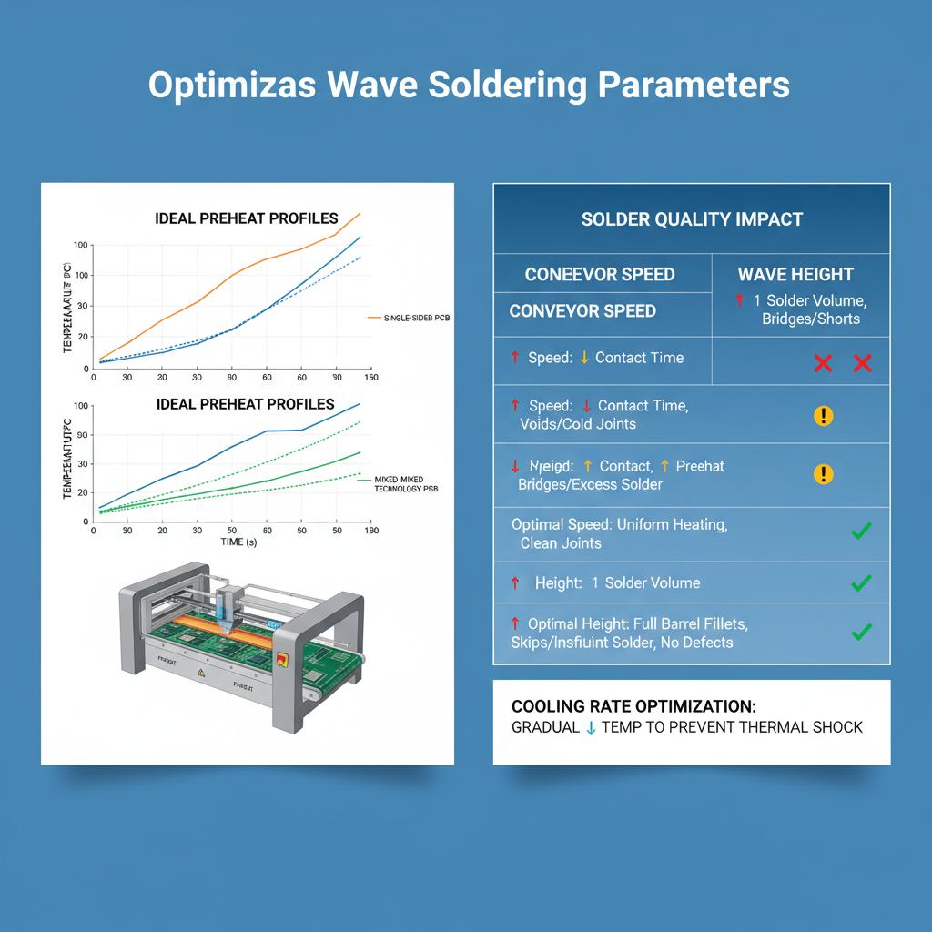
Wave soldering is a pivotal process in PCB assembly, and optimizing its parameters is essential for achieving superior performance and reliability. This section provides a detailed analysis of key parameters such as conveyor speed, preheat temperature profile, solder pot temperature, wave height, and wave contact time, offering practical guidance tailored to different PCB types and component characteristics.
Geschwindigkeit des Förderers
The conveyor speed is crucial as it influences the time components are exposed to the solder wave. For single-sided boards with larger components, a slower speed allows for better solder adhesion and minimizes the risk of solder bridges. Conversely, faster speeds may be implemented for double-sided boards or mixed technology assemblies where excess solder needs to be controlled to prevent clogging lead holes. For more detailed insights into conveyor systems and their optimization, you might find our article on Affordable PCB Conveyors helpful.
Preheat Temperature Profile
Preheating prepares the board and components for soldering by minimizing thermal shock. Ideal profiles differ based on PCB types and component sensitivity:
- Single-Sided PCB: Utilize a gradual ramp-up temperature to ensure uniform heating.
- Double-Sided or Mixed Technology: A steeper profile might be necessary to adequately heat components with higher thermal mass.
Adjusting the zone temperatures, particularly the peak temperature in the final zone, is vital to prevent component damage while ensuring the solder flows optimally. For those dealing with more complex soldering environments, consider the synergy between reflow ovens and chillers for precise temperature management, as discussed in our article on Reflow Ovens and Chillers.
Löttopf-Temperatur
The solder pot temperature must be calibrated to the type of solder and flux used, but generally falls within the range of 240°-265°C for lead-free solder. It’s important to ensure it is consistently maintained to prevent oxidation and achieve uniform wetting.
Wave Height
Wave height directly affects solder application quality. Adjustments should be made based on board thickness and component clearance:
- Thin Boards: Ensure lower wave height to avoid solder flooding.
- Thicker Boards: Increase wave height to promote adequate penetration through plated-through holes.
Wave Contact Time
This parameter should be optimized to match the thermal mass of components. Components with higher thermal mass require longer contact times for effective soldering.
Common Wave Soldering Defects: Identification, Causes, and Troubleshooting
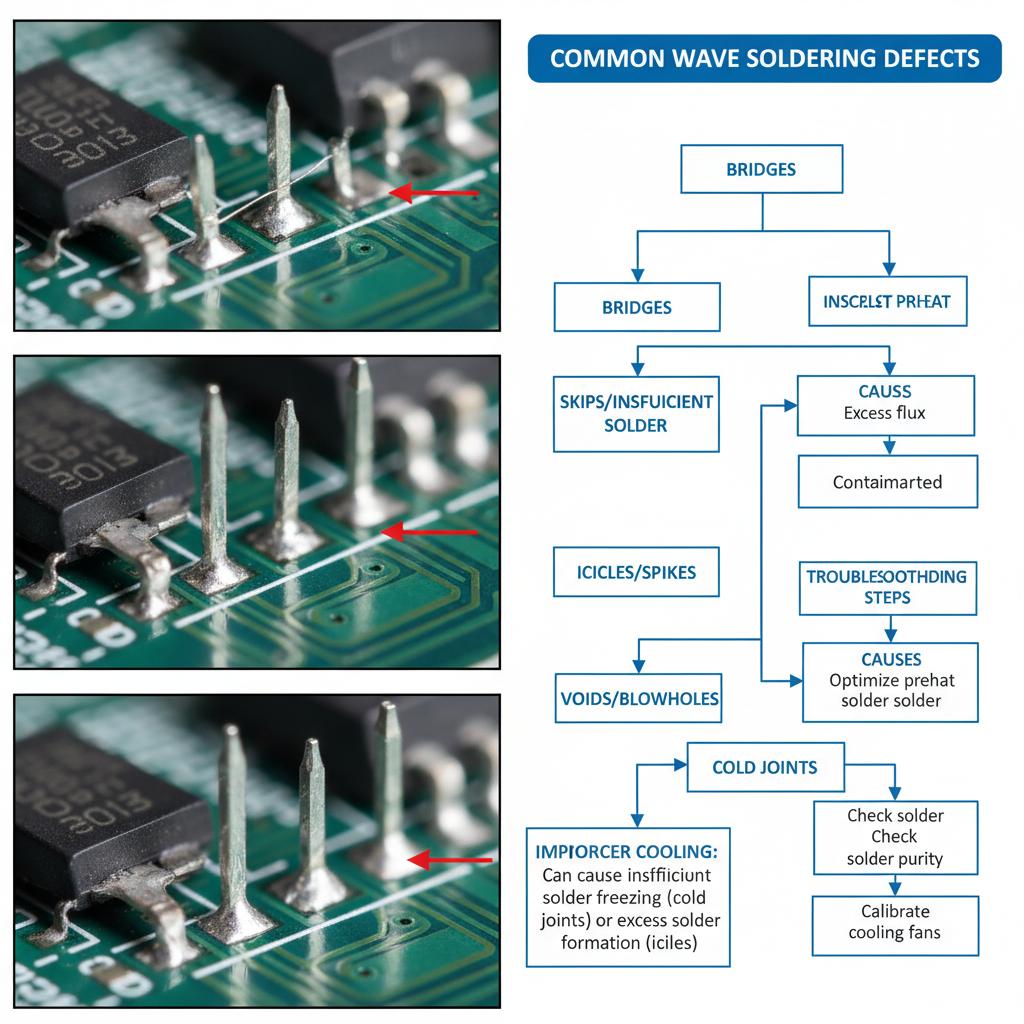
Wave soldering, while efficient for large-scale production, often presents a set of challenges primarily embodied in soldering defects. Understanding these defects, their origins, and remediation techniques is crucial for optimizing manufacturing reliability.
1. Bridges
- Visual Characteristics: Unintended solder linking component leads.
- Probable Causes: Incorrect conveyor angle, excessive solder temperature, or poor flux application.
- Fehlersuche: Adjust conveyor angle to ensure proper lead separation, fine-tune solder temperature settings, and verify flux adequacy.
For further reading on preventing solder bridging, check out our Comprehensive Guide to Preventing Solder Bridging in Wave Soldering.
2. Skips
- Visual Characteristics: Non-soldered pads or tracks left bare.
- Probable Causes: Insufficient fluxing, low preheat temperature, uneven solder wave height.
- Fehlersuche: Ensure thorough flux application, calibrate preheat settings, and maintain consistent wave height.
Improper cooling rates significantly contribute to defects such as voids and cold joints due to uneven solidification. Careful adjustment of cooling mechanisms, promoting uniform heat dissipation across components, can mitigate these issues.
Troubleshooting Flowchart
- Defect Identification: Visual inspection reveals defects.
- Initial Check: Confirm proper settings for machine parameters (temperature, wave height).
- Detailed Cause Analysis: Assess flux quality, conveyor speed, solder compositions.
- Systematic Adjustment: Methodical tweaking based on defect type.
- Result Verification: Re-inspect for defect resolution, iterate if necessary.
Quality Control and Inspection in Wave Soldering: Ensuring Reliability
In the realm of electronics manufacturing, where precision and reliability are paramount, robust quality control during the wave soldering process is not merely a best practice but a necessity. Ensuring the integrity of solder joints starts with meticulous inspection methods and adheres to stringent industry standards.
Maintenance and Calibration of Wave Soldering Machines
Maintaining and calibrating wave soldering machines is pivotal in ensuring optimal performance, extending their lifespan, and minimizing operational costs. Routine and periodic maintenance encompass cleaning, lubrication, and calibration tasks, which are essential to prevent downtime and ensure the quality of soldering operations.
Routine Maintenance Tasks
Begin with daily cleaning of the solder pot to prevent the buildup of oxidation by-products that can affect solder quality and machine efficiency. Regularly inspect and clean the fluxer and preheater; these areas accumulate residues that can lead to uneven heat distribution and flux application.
Lubrication of moving parts is also crucial. Ensure that conveyor components and other mechanical parts are regularly lubricated to avoid wear and tear, reducing the risk of breakdowns. For more guidance on maintaining conveyor components, you might find our guide to SMT conveyor belt replacement helpful.
Wave Soldering vs. Reflow Soldering: A Comparative Analysis
Wave soldering and reflow soldering are two fundamental techniques in electronics manufacturing, each with unique principles and applications. Understanding the differences between these methods provides critical insights into optimizing PCB assembly processes.
Principles and Suitable Applications
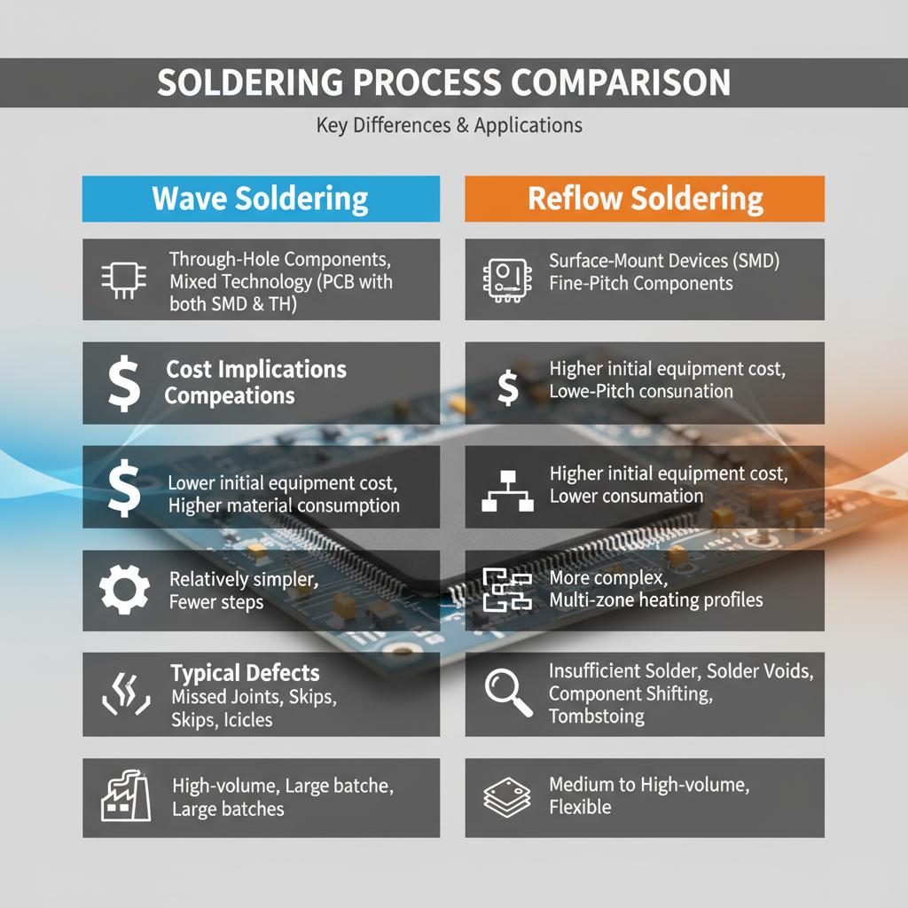
Wave soldering involves the process of passing PCBs over a wave of molten solder, primarily used for through-hole components. Reflow soldering, in contrast, utilizes heat to melt solder paste on the PCB, which is ideal for Surface Mount Devices (SMDs). Both methods can accommodate mixed technology boards. For an in-depth look at the reflow process, see A Comprehensive Guide To The SMT Reflow Oven Process.
Advantages and Disadvantages
Wave soldering is advantageous for high-volume production and its suitability for large, complex through-hole components. However, it faces challenges with miniaturization and precision compared to reflow soldering, which efficiently supports fine-pitch components and complex geometries.
The disadvantages of wave soldering include potential thermal stress and difficulty in handling SMDs without extra fixtures, while reflow soldering requires precise thermal profiling and control.
Equipment and Process Complexity
Wave soldering machines comprise fluxing, preheating, soldering, and cooling stages, which require consistent calibration for optimal results. Reflow soldering equipment, including reflow ovens, demands fine temperature control across multiple zones. To understand the critical role of equipment in soldering, refer to Wave Soldering Operation Guide.
The complexity of the wave soldering process lies in managing board orientation and solder coverage. Reflow soldering, while seemingly straightforward, involves intricate thermal profiling, where cooling rates significantly affect solder joint quality.
Typical Defects and Troubleshooting
Wave soldering defects often involve solder bridges, non-wetting, and icicles. Reflow soldering may encounter tombstoning or insufficient solder flow. Effective troubleshooting requires understanding the root causes, often tied to equipment calibration, flux quality, or temperature settings. For tips on preventing defects, see A Comprehensive Guide To Preventing Solder Bridging In Wave Soldering.
Cost Implications and Production Volumes
Considering cost, wave soldering is typically cheaper for high-volume runs due to its efficiency in handling multiple boards simultaneously. For lower volumes, reflow soldering may be more cost-effective because it provides better control and quality for intricate SMD assemblies.
Environmental Considerations and Safety in Wave Soldering
Wave soldering impacts various environmental and safety aspects within electronics manufacturing. Transitioning from leaded to lead-free soldering technologies is among the most significant environmental changes, driven by regulatory concerns and market demand for greener electronics. While lead-free solders eliminate toxic lead exposure, they introduce challenges such as higher melting temperatures which can affect machine calibration and manufacturing processes. For insights into maintaining proper machine operation temperatures, explore The Critical Role of Chillers in Reflow Oven Temperature Control.
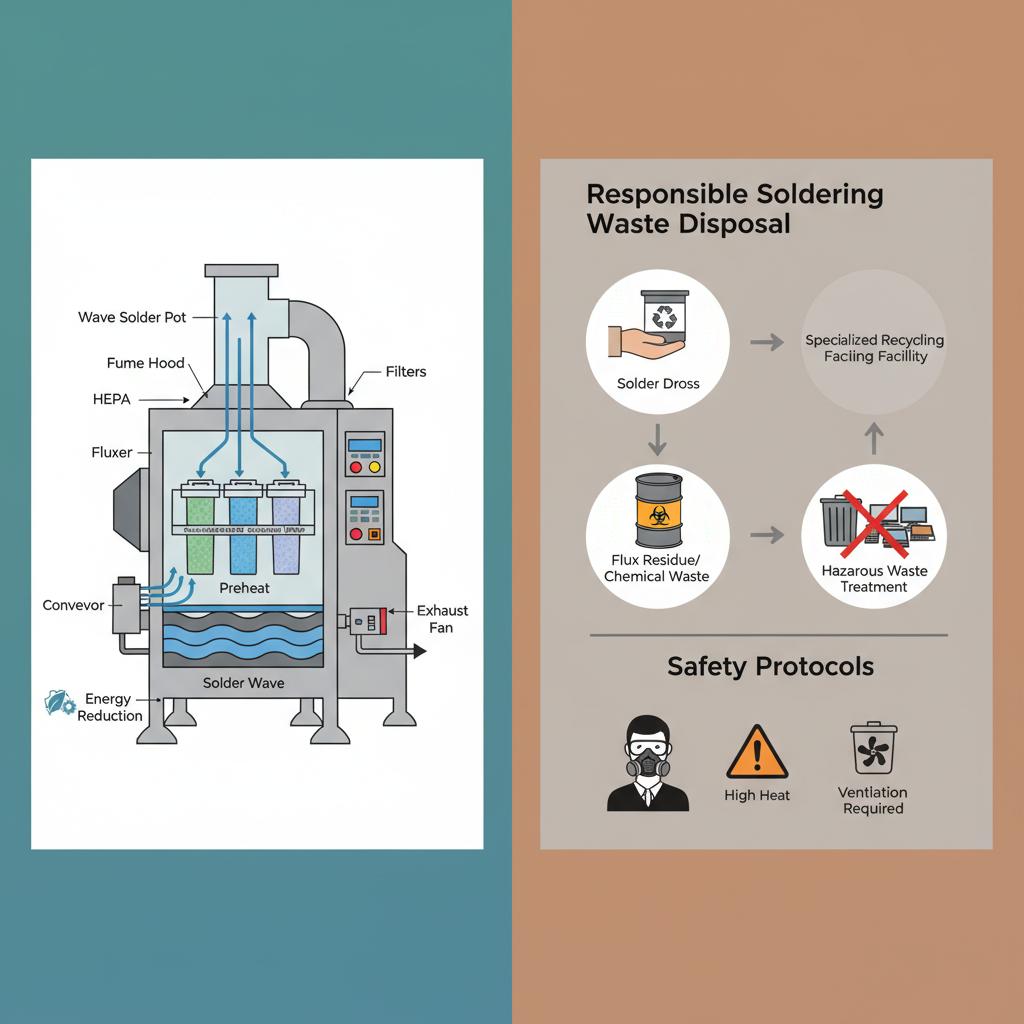
Effective flux waste disposal is crucial in wave soldering operations. Flux residue and dross, by-products of the soldering process, require proper management to minimize environmental contamination. Implementing responsible disposal practices, such as recycling and reuse programs, is essential for sustainable operations. Moreover, energy consumption in wave soldering machines is a primary concern due to constant operations involving heating and maintaining molten solder. Employing energy-efficient soldering equipment and optimizing machine usage can significantly reduce environmental impact.
Fume extraction systems are integral to maintaining air quality. Designed to remove harmful fumes generated during soldering, these systems ensure compliance with industrial hygiene standards. Proper function and maintenance of these systems are critical for both environmental health and worker safety.
Safety protocols in wave soldering emphasize handling molten solder, chemicals, and high temperatures. Workers must be equipped with personal protective equipment (PPE) including gloves, protective eyewear, and heat-resistant clothing to mitigate risks. Furthermore, adequate ventilation is necessary to prevent exposure to toxic fumes and maintain a safe working environment. Refer to our Wave Soldering Operation Guide for detailed operational insights and safety measures.
Integrating these environmental and safety considerations into wave soldering processes not only complies with industry standards but also enhances operational efficiency and workforce safety. Manufacturers are encouraged to adopt comprehensive strategies that prioritize these aspects, contributing positively to sustainable electronics manufacturing.
Emerging Trends and Future of Wave Soldering Technology
Wave soldering technology continues to evolve rapidly, shaped by advancements that cater to both efficiency and adaptability to modern electronic manufacturing demands. As the industry moves toward more sustainable and technologically integrated solutions, several key trends are emerging that redefine the capabilities and applications of wave soldering.
One significant advancement is in lead-free solder alloys, essential for compliance with environmental regulations such as RoHS. These alloys offer improved conductivity and reliability, crucial for evolving printed circuit board (PCB) designs that demand higher performance standards. In tandem, inert atmosphere soldering is gaining traction, where nitrogen or argon environments minimize oxidation and improve solder joint quality.
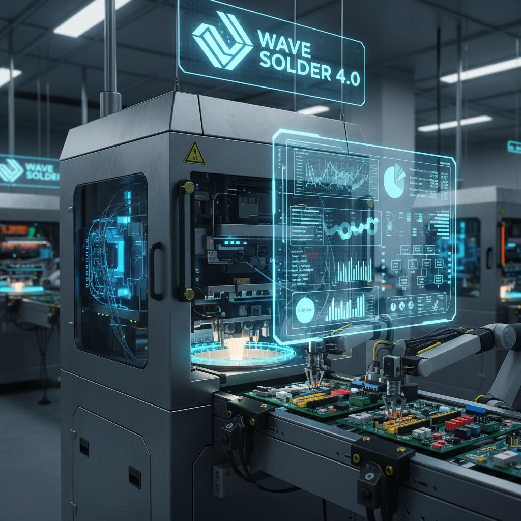
Selective wave soldering is another breakthrough, allowing manufacturers to precisely target specific areas on a PCB. This reduces waste and adapts to complex designs involving mixed technology boards. Coupled with intelligent control systems driven by Industry 4.0, wave soldering machines are increasingly integrated with sensors and data analytics. These innovations empower real-time monitoring and adjustments through AI and machine learning algorithms, optimizing the soldering process and minimizing defects.
Energy-efficient designs reflect an industry-wide shift towards sustainability, reducing operational costs while maintaining high performance. These designs focus on minimizing energy consumption without compromising on output quality, balancing economic and environmental benefits.
As components and PCB designs continue to evolve, wave soldering technology adapts to new challenges. The integration of flexible PCB materials and smaller, more intricate components requires advanced soldering techniques to maintain precision and reliability.
In conclusion, the future of wave soldering offers promising advancements that enhance its adaptability and efficiency. As manufacturers strive for greater production volumes at reduced costs, the synergy between wave and reflow soldering remains crucial. Consider exploring the Wave Soldering Operation Guide for insightful information on optimizing these processes. These trends invite stakeholders to explore visual aids and case studies to deepen understanding and implement best practices, ensuring wave soldering’s enduring role in electronics manufacturing.
Conclusion: The Enduring Role of Wave Soldering in Electronics Manufacturing
Wave soldering remains a cornerstone in electronics manufacturing, particularly for through-hole components and mixed-technology PCBs. This guide has delved into its intricate principles, components, process steps, and critical considerations for quality and optimization. From the foundational science to advanced troubleshooting, and from environmental stewardship to emerging technological trends, understanding wave soldering in depth is paramount for engineers and technicians in the field. By continuously refining parameters, implementing robust quality control, and embracing sustainable practices, the enduring role of wave soldering in producing reliable electronic assemblies is assured, paving the way for future innovations in electronics manufacturing.
