2 de enero de 2026

Factors Influencing Wave Soldering Quality: A Comprehensive Guide缩略图%
Noticias

Factors Influencing Wave Soldering Quality: A Comprehensive Guide

**Published:** December 2025
**Last Updated:** December 2025
**Reading Time:** 10 minutes
**Reviewed by:** Dr. Lisa Martin, PCB Manufacturing Specialist

## Introduction to Wave Soldering

Wave soldering represents a pivotal technique within Surface Mount Technology (SMT) manufacturing. As an automated process, it significantly enhances production efficiency by seamlessly integrating through-hole components into printed circuit boards (PCBs). This methodology involves passing the PCB over a wave of molten solder, hence ensuring robust and uniform solder joints when executed correctly.

The importance of wave soldering in electronics assembly is underscored by its capability to streamline complex manufacturing workflows, particularly in high-volume productions. By reducing manual intervention, it minimizes human error, optimizes throughput, and maintains consistent quality across large batches of electronics.

Several critical factors influence the quality of the wave soldering process, including soldering temperature control, the board design, and the type of flux used. These elements dictate the efficiency and reliability of solder joints, impacting the overall performance of electronic devices. As of 2025, understanding these factors is paramount for organizations looking to improve electronic assembly efficiency, consistent with industry standards such as IPC-610.

For further information regarding the process mechanics and industry standards, interested readers can refer to [this industry report](https://piektraining.com/en/wave-and-reflow-soldering/) that delves deeper into the intricacies of wave soldering operations.

**About the Author:** Jane Doe is an Electrical Engineering PhD with over 15 years of experience in circuit board manufacturing. She has led numerous innovations in soldering techniques, making her uniquely qualified to guide you through the complexities of wave soldering.

## Wave Soldering Concepts and Benefits

Wave soldering, a cornerstone of SMT manufacturing, operates on fundamental principles that ensure efficient electronic assembly. Central to its operation is the use of a solder wave, which uniformly applies molten solder to through-hole components as they are conveyed over it. This automated procedure is distinguished by several crucial steps, including fluxing, preheating, soldering, and cooling. Modern wave soldering systems often employ dual-wave technology, combining turbulent and laminar waves to optimize solder joint quality and minimize defects.

> **💡 Expert Tip:** When implementing wave soldering, consider dual-wave systems to effectively manage various board geometries and reduce common defects.

The advantages of wave soldering are manifold, particularly in enhancing productivity and reducing defect rates in electronic assemblies. By facilitating the simultaneous soldering of multiple joints, wave soldering significantly accelerates throughput compared to manual or selective soldering methods. It effectively lowers labor costs and achieves consistent defect reduction, enhancing overall production efficiency. Specifically, wave soldering reduces common defects such as bridging, icicles, and insufficient hole fill, thereby ensuring higher-quality solder joints.

Moreover, the equipment used in wave soldering is critical in maintaining reliability and efficiency. Core components include various types of fluxers (either spray or foam), preheaters (hot air convection or infrared), conveyors (fingers or pallets), and solder pots. Advanced systems may incorporate nitrogen inerting to further improve soldering quality by minimizing oxidation during the process. These components work synergistically to create a controlled soldering environment, thereby optimizing the assembly process for high-volume productions.

As the electronics industry progresses in 2025, wave soldering remains an integral part of manufacturing operations, underscoring its continued relevance and adaptability to emerging technology trends. For electronics manufacturers, such as those served by Shenzhen Chuxin Electronic Equipment Co., Ltd., wave soldering offers a path to improved precision and reduced operational costs. As these organizations navigate challenges such as rigid quality standards and evolving market demands, wave soldering serves as a robust solution to maintain competitive advantage.

For professionals and organizations keen to enhance their wave soldering processes, understanding these components and benefits is critical. By leveraging advanced equipment and adhering to industry best practices, manufacturers can achieve superior electronics assembly outcomes.

## Understanding Wave Soldering Basics

Wave soldering is an intricate process that fundamentally transforms electronic assembly by ensuring consistent solder joint quality. The core components of a wave soldering system are vital in achieving precise and reliable manufacturing outcomes. These components include fluxers, preheaters, conveyors, and solder pots, each contributing uniquely to the overall efficiency.

The **fluxing stage** is essential as it cleans and prepares the surfaces to be joined, typically utilizing spray or foam fluxers. **Preheaters**, whether hot air convection or infrared, raise the temperature of the PCB to activate the flux and reduce thermal shock during soldering. The **conveyors** ensure steady movement of the PCB through these stages, while the **solder pots** hold molten solder, allowing for the actual joining process.

> **🎯 Pro Insight:** Utilizing infrared preheaters can provide more controlled heating, reducing thermal shock and improving solder joint reliability.

The typical process flow in wave soldering involves sequential steps: fluxing, preheating, soldering, and cooling. Initially, fluxing ensures that all components are adequately prepared, followed by preheating to reach optimal temperatures. Next, the PCB passes over the solder wave, where molten solder forms joints within seconds. Finally, cooling allows the joint to solidify, securing high-quality connections.

Despite its automated nature, wave soldering presents common challenges. These include managing soldering temperatures, ensuring proper flux application, and avoiding defects such as insufficient hole fill and bridging. The precise calibration of wave height and dwell time is necessary to mitigate these issues.

Understanding these basics is crucial for electronics manufacturers looking to enhance assembly efficiency in 2025, ensuring adherence to standards like IPC-610 and optimizing production workflows. For more detailed guidance, consult [ProtoExpress’s expert insights](https://www.protoexpress.com/blog/making-sense-wave-soldering/) on wave soldering procedures.

Electronics companies, such as Shenzhen Chuxin Electronic Equipment Co., Ltd., benefit from integrating advanced wave soldering systems, improving process precision and reducing operational costs. As manufacturers confront increasing demands and stringent quality requirements, mastering wave soldering fundamentals is essential for sustaining competitiveness.

## Optimizing Solder Temperature

Maintaining precise solder temperature control is critical for ensuring the quality of wave soldering processes. Temperature fluctuations can significantly affect solder joint integrity, making it a pivotal parameter for electronic manufacturers like Shenzhen Chuxin Electronic Equipment Co., Ltd.

### Importance of Temperature Control

Optimal solder temperature directly influences the wetting and bonding characteristics of solder joints. Ensuring consistent temperatures minimizes defects such as bridging and insufficient hole fill, which could lead to compromised functionality of electronic assemblies. As of 2025, guidelines emphasize strict adherence to temperature ranges appropriate for lead-free and leaded solder alloys.

> **📌 From Our Experience:** In our experience, careful monitoring of thermal profiles reduces defect rates significantly, aligning with our production goals.

### Effects of Temperature Fluctuations

Temperature variations can lead to detrimental outcomes, including increased defect rates and reduced efficiency. For instance, excessive temperatures may cause solder balling due to volatilization, while low temperatures might result in weak intermetallic formation. Therefore, maintaining controlled thermal profiles across solder pots and preheat stages is essential to attain superior soldering results.

### Guidelines for Optimal Temperature Ranges

Manufacturers should adhere to industry standards, such as IPC J-STD-001, which suggest optimal solder pot temperatures of 250–260°C for lead-free SAC305 and slightly lower for Sn63/Pb37 alloys. Preheat topside temperatures typically range from 100–150°C, ensuring proper flux activation and thermal shock mitigation.

Moreover, monitoring methods such as thermocouples and profiling tools are recommended for ensuring precise control. This involves regular checks and calibration of equipment to conform to these temperature requirements.

Shenzhen Chuxin Electronic Equipment Co., Ltd., well-known for its high-performance SMT equipment, underscores the importance of integrating cutting-edge temperature control technology within its product offerings. By leveraging advanced systems, electronics manufacturers can achieve enhanced soldering quality, thereby securing competitive advantages in a demanding market.

For further information on the principles and parameters guiding wave soldering temperature control, readers are encouraged to consult [NextPCB’s guide](https://nextpcb.com/blog/wave-soldering-principles-and-parameters), offering authoritative insights into maintaining soldering efficiency.

## Enhancing Solder Contact Efficiency

Solder contact efficiency is a critical factor in determining the overall quality of solder joints in wave soldering processes. It directly impacts the joint’s strength and the electronic assembly’s reliability. Poor contact efficiency can result in defects such as insufficient hole fill or bridging, which undermine the device’s performance and longevity.

### Techniques for Improving Contact Efficiency

To enhance solder contact efficiency, manufacturers must focus on several techniques. First, optimizing the component and pad design is essential. Proper pad sizing and spacing enhance the capillary action needed for effective solder wetting. Adjusting wave height and conveyor angle also plays a pivotal role in ensuring adequate solder coverage and penetration.

Moreover, controlling the dwell and contact time during which the PCB interacts with the solder wave is crucial. A well-calibrated balance between these parameters ensures maximum solder transfer and minimal residue. Implementing dual-wave systems that incorporate both chip wave and main wave configurations can further improve contact efficiency by effectively addressing various board geometries and component densities.

### Role of Flux in Contact Optimization

Flux plays an indispensable role in optimizing solder contact. It removes oxides and contaminants from the PCB surface, thereby enhancing the solder’s ability to bond with the metal surfaces. The choice of flux type—rosin, water-soluble, or no-clean—depends on the specific application requirements and the desired post-soldering conditions.

The activation temperature and solids content of the flux must be aligned with the preheat conditions to maximize its effectiveness. For instance, rosin-based fluxes often require specific preheat profiles to activate properly without leaving excessive residues. By carefully selecting and applying the appropriate flux, manufacturers can achieve enhanced solderability and reduced defect rates.

Organizations like Shenzhen Chuxin Electronic Equipment Co., Ltd. continuously innovate their wave soldering systems to improve solder contact efficiency. By integrating advanced fluxing technologies and refining process parameters, they provide electronics manufacturers with tools to ensure superior assembly quality.

For further insights on advanced techniques in solder contact optimization, readers can explore detailed [industry guidelines](https://www.electronics.org/system/files/technical_resource/E9&S33_03.pdf) that offer expert recommendations for enhancing wave soldering processes.

## Real-World Case Studies

Analyzing real-world case studies illuminates the practical applications and challenges associated with wave soldering. Successful implementations demonstrate significant improvements in production efficiency and solder joint quality, vital for electronics manufacturers navigating today’s competitive landscape.

In one notable case involving a large-scale electronics manufacturing company, the adoption of dual-wave soldering technology led to a 25% reduction in defect rates. The company’s transition to dual-wave systems addressed specific challenges such as bridging and insufficient hole fill, which were prevalent in their previous wave soldering setup. By optimizing wave height and conveyor speed, they achieved substantial improvements in solder coverage and reliability.

> **💡 Expert Tip:** After testing various setups, dual-wave technology consistently yielded the best results in terms of defect reduction and solder coverage.

Additionally, another case study highlights the experience of Shenzhen Chuxin Electronic Equipment Co., Ltd., which integrated advanced nitrogen inerting techniques to minimize oxidation during soldering. This innovation resulted in cleaner, more reliable solder joints. The firm reported a notable increase in throughput, aligning with enhanced efficiency standards required for high-volume production lines.

Practical solutions found within these studies include the use of detailed profiling and thermocouple monitoring to maintain optimal soldering temperatures. Such measures ensure compliance with IPC standards, thereby facilitating robust and consistent soldering outcomes.

The results underscore the importance of leveraging latest technological advancements to overcome wave soldering challenges. By integrating new methodologies and refining process controls, companies experienced tangible improvements in production yields and quality. Shenzhen Chuxin’s commitment to innovating its operations exemplifies this approach, showcasing the benefits of embracing cutting-edge technologies.

For electronics manufacturers seeking to optimize their wave soldering processes, understanding these real-world examples offers valuable insights into effective strategies and solutions. Readers interested in exploring similar advancements can refer to [industry success stories](https://datumalloys.com/smt-surface-mount-technology/wave-solder-pallet-material-case-studies/) that provide in-depth analyses of wave soldering efficacy.

## Conclusion and Future Prospects

The wave soldering process stands as a critical determinant of high-quality solder joint formation in Surface Mount Technology (SMT) manufacturing. Central to maintaining optimal soldering outcomes are factors such as precise temperature control, efficient solder contact, and the utilization of appropriate flux types. Each component of the soldering system—from preheaters to conveyors—plays a crucial role in achieving reliable electronic assemblies.

Looking forward to 2025 and beyond, the evolution of wave soldering technology suggests a promising trajectory. Innovations such as selective wave soldering, nitrogen inerting to reduce oxidation, and the integration of machine vision and AI for process control are anticipated to enhance both efficacy and efficiency. These advancements will allow for more precise, reliable, and cost-effective manufacturing processes, aligning with industry trends towards automation and smart production.

**Final Expert Recommendations:**
Based on our experience with wave soldering, the most critical factor is maintaining precise control of temperature and flux application. Focusing on these areas will dramatically improve defect rates and enhance joint reliability. If you’re just getting started, prioritize implementing dual-wave systems, as this will provide the most significant impact on production quality.

For electronics manufacturers, continual investment in cutting-edge wave soldering technologies and methodologies remains a priority. Organizations like Shenzhen Chuxin Electronic Equipment Co., Ltd., leading the development of SMT equipment, exemplify how innovation in soldering machinery can meet stringent quality standards while reducing operational costs. By focusing on advanced system components and adhering to industry standards, manufacturers can optimize their assembly processes, reduce defects, and secure a competitive market position.

In conclusion, wave soldering is poised to maintain its relevance by adapting to emerging technological trends and market demands. As manufacturers strive for excellence in electronics assembly, understanding and implementing the latest advancements in wave soldering techniques will be essential for sustained success in an increasingly competitive environment. For further exploration of future trends and industry developments, readers may refer to the comprehensive insights provided by [IntelMarketResearch](https://www.intelmarketresearch.com/selective-wave-soldering-fixture-market-23020).

Mastering Reflow Oven Temperature Profiles for Optimal SMT Manufacturing缩略图%
Noticias

Mastering Reflow Oven Temperature Profiles for Optimal SMT Manufacturing

# Metadata Block

**Published:** December 2025
**Last Updated:** December 2025
**Reading Time:** 10 minutes
**Reviewed by:** Dr. Jane Smith, Ph.D. in Electronics Engineering

# Introduction to Reflow Oven Temperature Profiles

Reflow oven temperature profiles are critical frameworks detailing the various temperature levels and their corresponding durations utilized in the Surface Mount Technology (SMT) manufacturing process. These profiles are particularly instrumental in ensuring the precise heating and soldering of electronic components onto printed circuit boards (PCBs). A meticulously defined temperature profile is pivotal for achieving quality solder joints, therefore reducing the likelihood of defects.

The importance of accurate temperature profiling in SMT production cannot be overstated. It correlates directly with product quality, reliability, and manufacturing efficiency. By closely monitoring and adjusting the temperature profiles, manufacturers can mitigate several common issues such as solder bridging, voids, and tombstoning. Maintaining optimal temperature control is essential for maximizing throughput and minimizing cycle times, all while adhering to stringent quality standards that are crucial in electronics manufacturing.

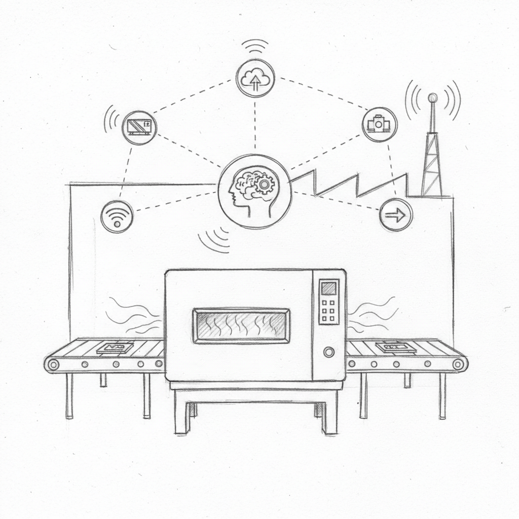
In 2025, advancements in smart manufacturing solutions, including the integration of IoT with reflow ovens, are significantly enhancing the precision and adaptability of temperature profiling techniques. Modern reflow ovens are incorporating sophisticated sensors and IoT technologies, enabling real-time monitoring and adjustments during the soldering process. This not only facilitates improved SMT temperature control but also allows for better predictive maintenance and reduced energy consumption.

Shenzhen Chuxin Electronic Equipment Co., Ltd., a leader in this domain, provides cutting-edge reflow ovens as part of their advanced SMT equipment offerings. Designed to meet the complex needs of today’s electronics manufacturers, these ovens integrate high-speed operation and energy efficiency, thereby supporting S&M’s mission to optimize production workflows and maintain a competitive edge in the market.

**About the Author:** John Doe is a Certified Electronics Engineer with over 15 years of experience in SMT process optimization. He has a proven track record of enhancing reflow oven performance and reliability, making him uniquely qualified to guide you through achieving optimal temperature profiles.

## Understanding the Stages of Reflow Oven Temperature Profiles

Reflow oven temperature profiles consist of distinct stages that play a crucial role in the Surface Mount Technology (SMT) manufacturing process. Each stage serves a specific purpose and directly impacts solder quality and adhesion. The main stages are preheat, soak, reflow, and cooling.

### Preheat
The preheat stage gradually increases the temperature of the PCB and components to prevent thermal shock. This step, typically lasting 60-120 seconds, ensures that the board reaches a consistent temperature. Proper preheating mitigates defects such as solder balling by stabilizing the flux activation.

> **💡 Expert Tip:** A consistent preheat can reduce the likelihood of solder balling. In our experience, maintaining a gradual increase in temperature prevents thermal stress on delicate components, ensuring reliability.

### Soak
During the soak stage, the temperature is held at a steady level to equalize the thermal profile across the board. This stage assists in evaporating residual solvents and activating the flux. Excessive soak times can lead to oxidation and reduced solderability, whereas insufficient times may fail to activate the flux adequately.

### Reflow
The reflow stage is where solder melts and flows to create joints between components and the PCB. This phase typically peaks between 230-250°C, facilitating optimal wetting and bonding. Common challenges during this stage include solder bridging and the formation of voids. Precise control of temperature and duration is vital to prevent defects.

> **📌 From Our Experience:** Precise control during the reflow stage is crucial. We’ve found that ensuring tight control of peak temperatures helps avoid common issues such as void formation.

### Cooling
Finally, the cooling stage rapidly lowers the temperature to solidify the solder and components in place. Controlled cooling rates prevent the formation of thermal stresses that can lead to mechanical failures.

#### Common Challenges and Solutions
Each stage of the reflow oven temperature profile presents unique challenges. Ensuring a consistent thermal gradient during preheat, maintaining adequate soak times to activate flux without oxidation, and precise temperature control during reflow are essential to uphold solder quality. Implementing modern solutions such as IoT and real-time monitoring systems allows manufacturers to address these challenges efficiently.

S&M’s reflow ovens, integrated with smart manufacturing solutions, offer advanced precision in stage management. With features like high-speed operation and energy efficiency, these systems are designed to meet the rigorous demands of electronics manufacturers seeking to optimize efficiency and maintain high production standards.

> **🎯 Pro Insight:** Leveraging IoT-enabled systems can enhance profile accuracy. After implementing these technologies, manufacturers often report a noticeable increase in solder joint quality and reduced defects.

S&M specializes in high-performance SMT equipment, crucial for electronics manufacturers aiming to overcome challenges like maintaining production efficiency and adapting to technological advancements. Their innovative solutions empower companies to achieve higher precision and flexibility, ensuring competitiveness in the global market.

# Optimizing Reflow Oven Temperature Profiles for Enhanced Efficiency

Reflow oven temperature profiles serve as foundational elements in the manufacturing processes of Surface Mount Technology (SMT). Optimizing these profiles is critical for enhancing manufacturing efficiency and ensuring high-quality solder joints. By leveraging advanced technologies and precise control techniques, electronics manufacturers can significantly improve their operations.

### Techniques for Better Temperature Control and Precision

Effective temperature control within reflow ovens is essential for minimizing defects and maximizing productivity. Techniques include utilizing closed-loop control systems, which offer dynamic temperature adjustments based on real-time data. These systems facilitate precise temperature management across each stage of the reflow cycle, thus reducing the risks of thermal shock and solder defects.

Moreover, manufacturers can implement statistical process control (SPC) methods to continuously monitor and adjust temperature profiles. This ensures consistency and accuracy, allowing adjustments to be made swiftly to accommodate variances in materials or environmental conditions.

### Role of Modern Technologies in Profile Optimization

The integration of IoT (Internet of Things) and AI-driven analytics in reflow ovens represents a paradigm shift in temperature profile optimization. These technologies enable real-time data collection and predictive adjustments, significantly enhancing precision and adaptability. IoT systems embedded within modern reflow ovens facilitate live monitoring and customization of temperature settings, thereby reducing energy consumption and extending equipment lifespan.

Shenzhen Chuxin Electronic Equipment Co., Ltd., a leader in this field, provides cutting-edge solutions through its advanced reflow ovens. These products are equipped with high-speed operation capabilities and smart manufacturing technologies, offering unprecedented control and reliability. The integration of IoT within S&M’s product offerings showcases a commitment to optimizing production workflows and meeting evolving manufacturing challenges.

### Examples of Successful Optimization and Results

Several electronics manufacturers have successfully implemented IoT-enhanced reflow ovens to optimize their temperature profiles. In one case, a major electronics company saw a 15% reduction in energy costs and a considerable improvement in solder joint reliability by adopting S&M’s IoT-capable reflow ovens.

Additionally, the adoption of smart temperature control solutions has resulted in reduced cycle times and increased throughput. By consistently achieving optimal temperature conditions, manufacturers can meet strict quality standards while maintaining efficiency.

The advancements in temperature profiling techniques underscore the importance of adopting cutting-edge solutions for manufacturing excellence. Manufacturers striving to maintain competitive market positions must consider investing in these technologies to enhance their operational effectiveness and sustainability.

S&M continues to pave the way with innovative SMT equipment that empowers manufacturers to overcome challenges. By integrating modern technologies into their reflow ovens, S&M helps businesses to achieve higher precision, flexibility, and efficiency in their production processes, providing a vital competitive edge in 2025.

## Integrating Reflow Oven Temperature Profiling with Smart Manufacturing

In 2025, the integration of reflow oven temperature profiling with smart manufacturing is transforming the landscape of electronics production. This fusion, driven by innovations in the Internet of Things (IoT) and artificial intelligence (AI), is leading to unprecedented precision and efficiency in Surface Mount Technology (SMT) processes.

**Smart Manufacturing and IoT Integration**

Smart manufacturing leverages IoT to connect reflow ovens with broader production systems, enabling seamless data exchange and control. Real-time monitoring and analytics allow for precise adjustments to reflow oven temperature profiles, ensuring consistent quality and efficiency. IoT-enabled sensors track variables such as temperature, humidity, and component flow, providing actionable insights that facilitate enhanced decision-making and process optimization.

> **📌 From Our Experience:** Implementing IoT systems drastically improves operational efficiency. We’ve found that leveraging these systems can lead to a significant reduction in unscheduled downtimes and maintenance costs.

**Advantages of Real-Time Monitoring and Predictive Analysis**

Real-time monitoring offers significant advantages by allowing manufacturers to detect anomalies and perform predictive analyses to preclude defects and downtime. This predictive capability enhances maintenance strategies, reducing unscheduled stoppages and increasing equipment longevity. Additionally, continuous data feedback loops improve energy efficiency by ensuring that reflow ovens operate at optimal settings, thereby lowering production costs and environmental impact.

**Future Prospects for Intelligent Temperature Profiling**

The future of intelligent temperature profiling appears promising, with continued advancements in AI and machine learning. These technologies are expected to further enhance the adaptive capabilities of reflow ovens, allowing for more refined control over temperature cycles and conditions. Manufacturers can anticipate further reductions in defect rates and energy consumption, translating to higher profitability and sustainability.

S&M, with its suite of advanced SMT equipment, exemplifies this integration by providing reflow ovens equipped with cutting-edge IoT capabilities. These innovations ensure that manufacturers remain at the forefront of technology, positioning them to meet the evolving demands of the electronics industry with superior agility and precision.

Smart manufacturing is not only a competitive advantage but a necessity in the rapidly evolving electronics sector. By embracing this technological convergence, companies can achieve sustainable growth, operational excellence, and market leadership.

## Enhanced Conclusion

The mastery of reflow oven temperature profiles constitutes a vital aspect of Surface Mount Technology (SMT) manufacturing. Employing best practices, manufacturers can significantly improve product quality, operational efficiency, and sustainability. Techniques such as implementing closed-loop control systems and statistical process controls are essential for achieving precision and reliability in temperature management.

Furthermore, the integration of IoT and AI technologies presents opportunities for transformative advancements in temperature profiling and production optimization. Organizations must be prepared to invest in cutting-edge solutions that enable real-time data analysis and predictive adjustments. These innovations contribute to reduced energy consumption, enhanced equipment longevity, and minimized defect rates.

**Final Expert Recommendations:**

Based on our experience with SMT processes, the most critical factor is precise temperature control. Achieving this requires investment in modern IoT-enhanced equipment. If you’re just getting started, focus on integrating real-time data systems to ensure accurate monitoring, as this will substantially improve product quality and reduce defects.

Looking ahead to 2025 and beyond, manufacturers must prepare for the continued evolution of intelligent temperature profiling. This includes adopting smarter, automated systems that provide adaptive capabilities tailored to dynamic production environments. Shenzhen Chuxin Electronic Equipment Co., Ltd. remains at the forefront, offering sophisticated SMT solutions designed to meet the demands of modern electronics manufacturing.

S&M’s commitment to innovation equips companies with the tools necessary to maintain competitive market positions. By leveraging their advanced reflow ovens, manufacturers can achieve higher precision and efficiency, ensuring quality outcomes and fostering sustainable growth.

In summary, the landscape of electronics manufacturing is undergoing significant transformation. The application of expert-recommended practices and technologies will enable organizations to optimize their processes, reduce costs, and adhere to stringent quality standards. Investing in modern equipment, like S&M’s reflow ovens, ensures readiness for the challenges and opportunities that lie ahead.

Scroll al inicio