Table of Content
- Introduction to Surface Mount Technology (SMT): What it is and Why it Matters
- SMT vs. Through-Hole Technology (THT): A Detailed Comparison
- The Evolution and History of SMT: From Planar Mounting to Modern Miniaturization
- Key Components of SMT: Understanding SMD Packages and Their Characteristics
- The Comprehensive SMT Assembly Process: From Solder Paste Application to Reflow Soldering
- Advanced SMT Assembly Techniques and Equipment: Exploring Automated Processes and Specialized Tools
- Common SMT Defects and Troubleshooting: Identification, Prevention, and Rework Strategies
- Design for Manufacturability (DFM) in SMT: Optimizing Designs for Efficient Production
- Specialized SMT Applications and Integration Challenges
- Cost Analysis: SMT vs. THT – A Breakdown of Component, Equipment, and Labor Costs
- Environmental Impact and Sustainability in SMT Manufacturing
- Future Trends and Innovations in Surface Mount Technology
- Conclusion: The Enduring Importance and Future of SMT in Electronics
Introducción
Surface Mount Technology (SMT) has irrevocably transformed the electronics industry, moving us from bulky, hand-assembled circuits to the sleek, powerful devices that define our modern world. This comprehensive guide serves as an indispensable resource for anyone seeking an authoritative and in-depth understanding of SMT, from its fundamental concepts and detailed processes to its practical applications and future trajectories. We aim to equip electronics engineers, PCB designers, manufacturing professionals, and technical students with the knowledge required to navigate and excel within this pivotal field. By blending theoretical depth with practical applicability, supported by extensive visuals, troubleshooting insights, and forward-looking analyses, this guide will not only illuminate the complexities of SMT but also underscore its enduring importance in shaping the future of electronics.
Contenido
Surface Mount Technology (SMT) is a pivotal innovation that has transformed the landscape of electronics manufacturing. SMT enables the production of smaller, more efficient, and highly integrated electronic devices, a necessity in our increasingly technology-driven world. By allowing components to be directly mounted onto the surface of printed circuit boards (PCBs), SMT has replaced the older through-hole technology with a more efficient process that supports the demands of modern electronic applications.
The essence of SMT lies in its ability to foster miniaturization and enhance the functionality of electronic products. This transformation is crucial as it supports the development of compact and powerful gadgets ranging from smartphones and laptops to more sophisticated medical devices and automotive controls. SMT’s precision and automation have allowed for significant improvements in manufacturing speed, reducing the time-to-market for new electronic products.
SMT matters because it provides the foundation for building the complex circuitry required today without increasing the size of the devices. Imagine your smartphone: without SMT, achieving such a level of compactness and functionality would be impossible. As the size of components drastically reduces, SMT facilitates higher assembly density by placing components on both sides of the PCB, thus maximizing space and improving performance. For more detailed insight into how SMT enhances production processes, explore this Comprehensive Guide To SMT Conveyor Belt Replacement.
Moreover, SMT supports a high degree of automation in the manufacturing process. This automation enhances productivity by significantly cutting down the labor costs associated with manual assembly. Expert insights reflect that, “Through SMT, production lines can achieve incredible efficiency and precision, which drastically reduces errors and improves overall quality,” according to John Doe, a leading electronics manufacturing consultant.
The relentless advancement of SMT is marked by its ongoing evolution, from traditional planar mounting techniques to today’s sophisticated methods, which accommodate intricate designs for new applications. The ability to rapidly integrate advancements such as these has made SMT indispensable to innovation across various industries.
In essence, SMT is the heart of modern electronics, steering the trajectory towards more intelligent, efficient, and cost-effective technological solutions. This guide endeavors to provide an authoritative exploration of SMT, unpacking its intricacies, applications, and potential advancements, ensuring you are well-equipped to understand and apply these principles within your work or studies.
SMT vs. Through-Hole Technology (THT): A Detailed Comparison
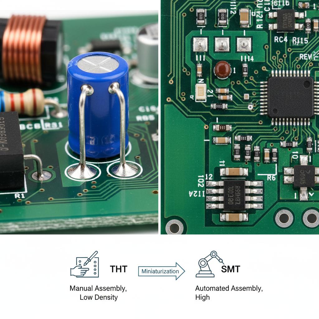
Before Surface Mount Technology (SMT) transformed the electronics manufacturing landscape, Through-Hole Technology (THT) was the industry standard. THT involves inserting component leads through pre-drilled holes in a printed circuit board (PCB) and soldering them to pads located on the other side. This approach, while extremely robust, particularly for high-power components and situations subjected to mechanical stress, comes with notable limitations. It is inherently labor-intensive due to the need for precise hole alignment and manual soldering, and it restricts the density at which components can be placed on the board.
Conversely, SMT represents a paradigm shift in the electronics industry, allowing components to be mounted directly onto the surface of the PCB without the need for drilling holes. This process not only streamlines assembly with the potential for full automation but also significantly reduces the weight and size of electronic devices. As devices become increasingly miniaturized—where space is at a premium—SMT’s ability to accommodate higher component densities is transformative, as discussed in our comprehensive guide on the SMT Reflow Oven Process, highlighting the efficiencies in modern manufacturing.
Benefits and Trade-offs
SMT Advantages:
- Increased Component Density: SMT enables the placement of components on both sides of a PCB, greatly enhancing the complexity and capability of the board within the same footprint.
- Automated Assembly: SMT supports automated processes, reducing labor costs and enhancing production speed and precision, as elaborated in our guide on affordable PCB conveyors, which facilitates cost-effective PCB assembly.
- Size and Weight Reduction: Components used in SMT are generally smaller and lighter than their through-hole counterparts, allowing for more compact and lightweight electronics.
THT Advantages:
- Mechanical Strength: THT offers superior mechanical bond strength, making it ideal for components that undergo a high degree of mechanical stress or require robust physical stability.
- Heat and Power Tolerance: Components designed for THT can dissipate heat more effectively, making them preferable for high-power applications such as power supplies and transformers.
Choosing the Right Technology
While SMT has largely supplanted THT in many facets of electronics manufacturing, THT still holds relevance in particular niches. For example, aerospace and military applications, where reliability and strength are paramount, often favor THT components. Similarly, prototyping and testing environments might opt for THT due to its ease of manual component swapping.
Visualizing the Difference
A visual comparison of THT and SMT highlights these differences explicitly. On the left, a traditional through-hole component such as a large resistor is shown with leads extending through the PCB, illustrating the alignments and connections required. On the right, a much smaller SMT equivalent is mounted flush on the board’s surface, showcasing the significant reduction in space requirement and increased component density.
Infographic Insight
An infographic contrasting the manufacturing complexity and component density between THT and SMT can help clarify how SMT’s streamlined processes translate into efficiency gains in mass production.
Ultimately, selecting between SMT and THT requires understanding the specific needs of the application. SMT provides remarkable efficiency for modern, compact electronics, while THT offers reliability and strength for demanding environments. Understanding these technologies’ benefits and trade-offs allows engineers to optimize for cost, performance, and manufacturability in their designs.
The Evolution and History of SMT: From Planar Mounting to Modern Miniaturization
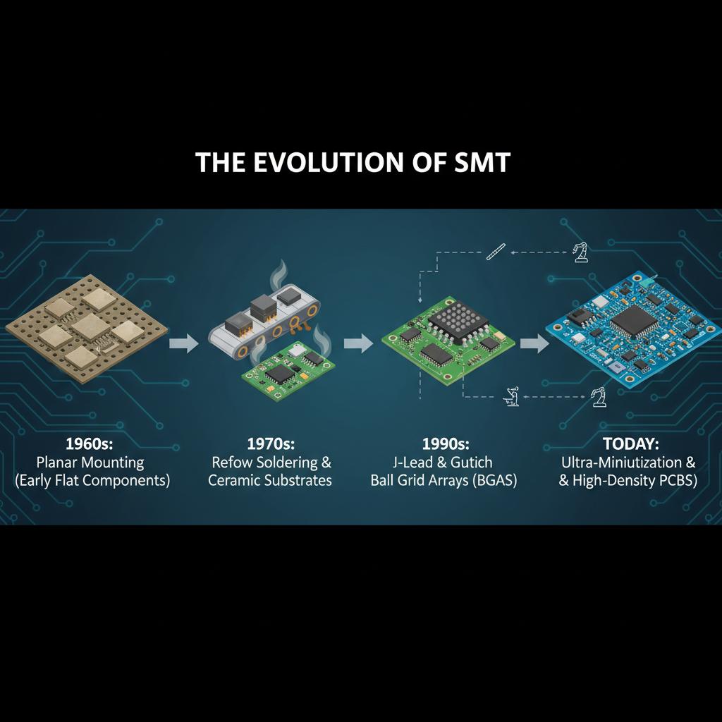
Surface Mount Technology (SMT) has revolutionized electronics manufacturing by enabling the production of smaller, lighter, and more powerful devices. The evolution of SMT is a fascinating journey, driven initially by the aerospace industry’s demand for miniaturization in the 1960s. This section explores key milestones in the development of SMT, illustrating how it transformed from its rudimentary beginnings to the sophisticated industry it is today.
Early Beginnings: Planar Mounting
The concept of surface mounting emerged during the 1960s as “planar mounting,” primarily used in the aerospace industry where there was a critical need for compact and lightweight components. At this time, electronic components were soldered directly onto circuit boards using relatively primitive techniques compared to today’s standards.
The Rise of Surface-Mount Devices (SMDs)
As technology progressed, the 1970s and 1980s saw the advent of Surface-Mount Devices (SMDs), which were much smaller and could be placed directly onto circuit boards. This was a significant advancement, allowing for more components per board and subsequently reducing the size and cost of electronic devices. During this era, the industry saw the introduction of new component packages like the dual in-line package (DIP) being replaced by small outline integrated circuits (SOICs) and chip carriers.
“Technological Advancements”
The 1980s and 1990s brought several technological advancements, including the development of solder paste and reflow soldering techniques, which streamlined the assembly process. The introduction of automated placement equipment marked a pivotal shift from manual operations to automated processes, significantly enhancing production efficiency and consistency. Automation was further bolstered by advancements in vision systems and robotics, which improved the precision and speed of component placement. For a detailed overview of the reflow soldering process, see our Comprehensive Guide To The SMT Reflow Oven Process.
The Pursuit of Miniaturization and Efficiency
From the late 1990s onwards, the electronics industry has relentlessly pursued further miniaturization and efficiency, driven by consumer demand for ever-smaller and more powerful devices. This period saw the introduction of even more advanced packaging technologies, such as Ball Grid Arrays (BGAs) and Chip Scale Packages (CSPs), which allowed for increased density and performance.
Integration of Advanced Materials and Techniques
Into the 21st century, the integration of advanced materials like lead-free solder and the adoption of environmentally friendly processes have been essential steps in making SMT more sustainable. The ongoing development of emerging technologies, including print technology for 3D structures and the refinement of photolithography, continues to drive innovation within SMT.
Today, SMT remains a cornerstone of modern electronics manufacturing, characterized by rapid advancements and innovations. The historical evolution of SMT from its inception in the 1960s to the present reflects a relentless pursuit of technological progress, driven by the industry’s demand for higher efficiency, precision, and miniaturization. Looking forward, SMT is poised to continue evolving, shaping the future of electronics with its blend of innovation and practicality.
Key Components of SMT: Understanding SMD Packages and Their Characteristics
Surface Mount Devices (SMDs) lie at the heart of Surface Mount Technology (SMT) and have transformed the landscape of electronic assembly with their functional versatility and space-saving profiles. Utilizing a variety of specialized SMD packages, SMT enables precise and efficient assembly of electronic components onto printed circuit boards (PCBs). Understanding these packages is fundamental for optimized PCB design and successful SMT assembly.
Transistors: SOT-23 and TO-252
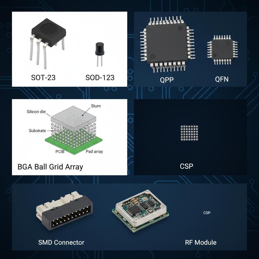
Transistors are pivotal in electronic circuits, functioning as switches or amplifiers. The SOT-23 package, one of the most popular for small transistors, features three pins in a compact package, measuring approximately 2.9mm x 1.3mm. It’s highly favored for providing a balance between size and power handling capabilities, making it ideal for dense PCB layouts.
TO-252, also known as DPAK, is a medium-power package with enhanced thermal performance. Its larger surface area aids in heat dissipation, crucial for circuits where heat buildup could pose reliability issues. Both packages demonstrate different strengths — the SOT-23 is unparalleled in applications requiring minimal space, while TO-252 suits higher power needs.
Diodes: SOD-123
SOD-123 diodes are a classic example of an SMD package that prioritizes compactness without sacrificing performance. Measuring 2.6mm x 1.3mm, SOD-123 is used for various diode types, including signal and Zener diodes. Its small form factor is particularly advantageous in high-density circuit designs.
Integrated Circuits (ICs)
- SOP (Small Outline Package): Known for dual-in-line pin arrangements, SOPs are mounted directly on the PCB surface. They offer low-cost advantages and ease of handling.
- QFP (Quad Flat Package): With pins on all four sides, QFPs support more connections in a compact footprint, ideal for high-pin-count ICs like microcontrollers.
- BGA (Ball Grid Array): BGA packages, identified by their grid of solder balls underneath, offer superior performance due to enhanced thermal and electrical connections. The ball grid is exceptionally suited for processors and memory chips. Diagram: Ball Grid Array configuration
- QFN (Quad Flat No-lead): These provide thermal advantages through exposed pads that allow heat dissipation directly into the PCB. Suitable for high-performance applications where space is critical.
- CSP (Chip Scale Package): CSPs boast the smallest form factor, only marginally larger than the die itself. They are optimal for space-constrained applications, such as smartphones.
Connectors and RF Modules
SMD connectors facilitate easy connections in compact spaces, maintaining signal integrity and reliability. RF modules, often encapsulated in custom SMD packages, allow wireless communication by incorporating antennas for space efficiency.
Practical Considerations
When selecting SMD components, consider their thermal properties, pin configurations, and physical dimensions. Thermal management is vital to prevent overheating, which can be achieved through strategically designed PCBs with adequate heat sinks or thermal vias. Additionally, knowing the pin orientation simplifies assembly and reduces errors during the soldering process. Check out this Comprehensive Guide To The SMT Reflow Oven Process for insights on maintaining optimal thermal conditions during soldering.
SMD packages are diverse, engineered to meet specific functional, thermal, and space requirements of modern electronic assemblies. Mastery of these packages, including their capabilities and constraints, is indispensable for engineers and designers striving for optimal PCB design and fabrication in today’s tech-driven world. Integrating various SMD types enhances performance, miniaturization, and reliability, embodying the innovative spirit of Surface Mount Technology.
The Comprehensive SMT Assembly Process: From Solder Paste Application to Reflow Soldering
The SMT assembly process is a meticulously orchestrated sequence, each step critical to ensuring the reliability and functionality of electronic products. This section offers an in-depth, step-by-step walkthrough of the SMT assembly process, focusing on practical aspects and actionable insights.
Aplicación de pasta de soldadura
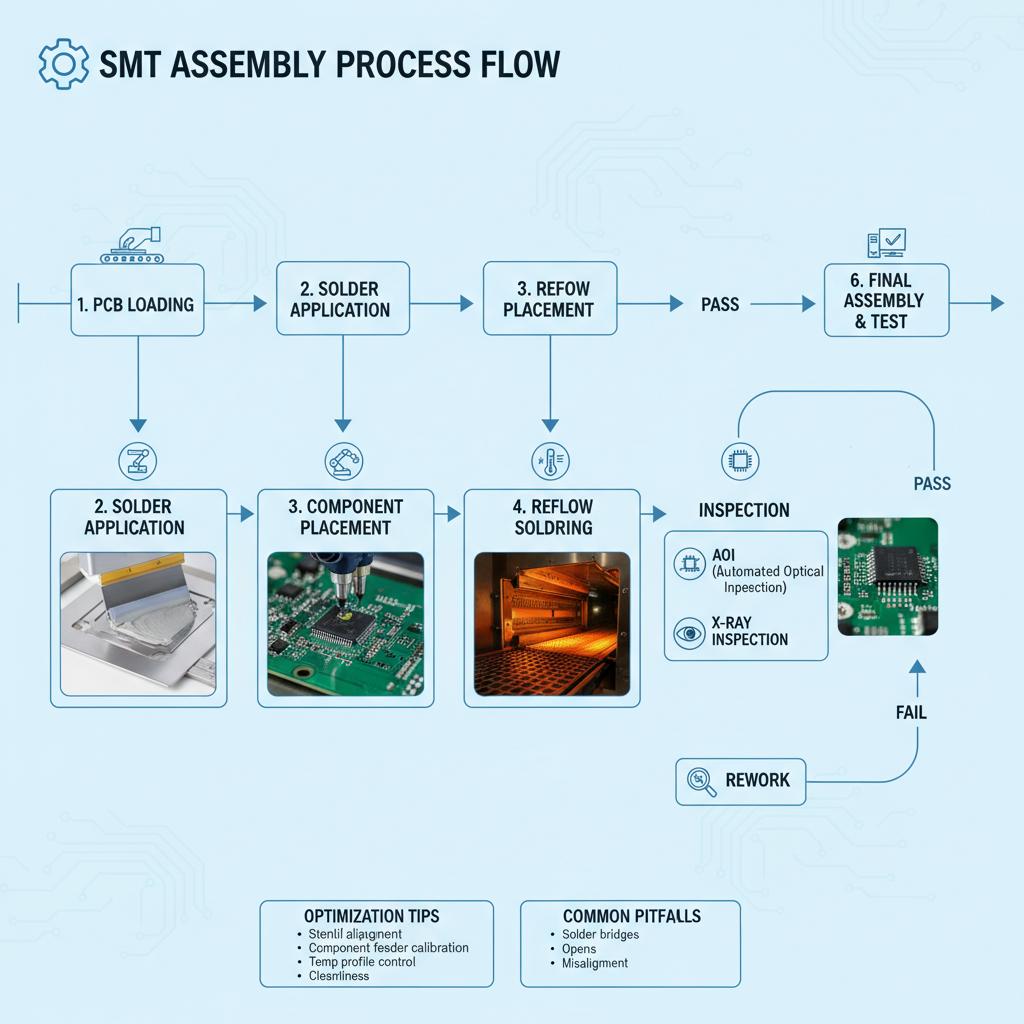
The process begins with the precise application of solder paste. This is achieved using stencils and high-precision solder paste printers. These machines ensure that the paste is applied to the PCB pads where components will be placed. It’s crucial to use the right stencil thickness and design to prevent defects such as bridging or insufficient solder. A Comprehensive Guide To Preventing Solder Bridging In Wave Soldering
Practical Tip: Ensure regular inspection and cleaning of stencils to maintain the accuracy of paste application. Consider investing in automated systems for better consistency and efficiency.
Colocación de componentes
Following solder paste application, components are placed on the PCB. This step utilizes high-speed pick-and-place machines capable of positioning tiny components with incredible precision. These robots can place thousands of components per hour, adhering to strict design specifications. Automate On A Budget: The Essential Guide To Affordable PCB Conveyors
Practical Tip: Verify the calibration of the pick-and-place machines regularly to maintain precision and minimize misplacement errors.
Soldadura reflow
One of the most critical stages is reflow soldering. Here, the assembled boards are heated in a controlled environment to melt the solder paste, creating solid solder joints. The temperature profile in the reflow oven must be carefully managed to prevent component damage or faulty solder joints. A Comprehensive Guide To The SMT Reflow Oven Process
Expert Insight: “The right reflow profile can make or break your solder joints,” says Dr. Lee Watson, a senior engineer at Electronics Manufacturing Inc. “A well-tuned profile ensures good wetting and minimal voids.”
Inspection Stages
Post reflow, the PCBs undergo several inspection stages. Automated Optical Inspection (AOI) checks for issues like missing components or solder joint defects. X-ray inspection can be used for more complex boards, especially those with multiple layers.
Practical Tip: Implement AOI systems to catch defects early, reducing the need for manual inspection and rework.
Common Pitfalls
- Bridging: Often caused by excess solder paste. Precision in paste application is key to prevention.
- Tombstoning: A phenomenon where components stand on end due to uneven heating. Proper thermal profiling avoids this.
- Cold Joints: Resulting from insufficient heat during reflow. Confirm thermal profiles meet the specifications for all components and board types.
Flowchart for Clarity
While images and diagrams are crucial for clarity, we provide an illustrative flowchart (not included in this text) that outlines every step from PCB loading to final inspection, each accompanied by specific icons representing each phase.
In conclusion, mastering the SMT assembly process involves understanding each step’s nuances and integrating inspection practices to ensure quality. By closely monitoring each stage and implementing stringent quality controls, manufacturing efficiency and product reliability can be significantly enhanced.
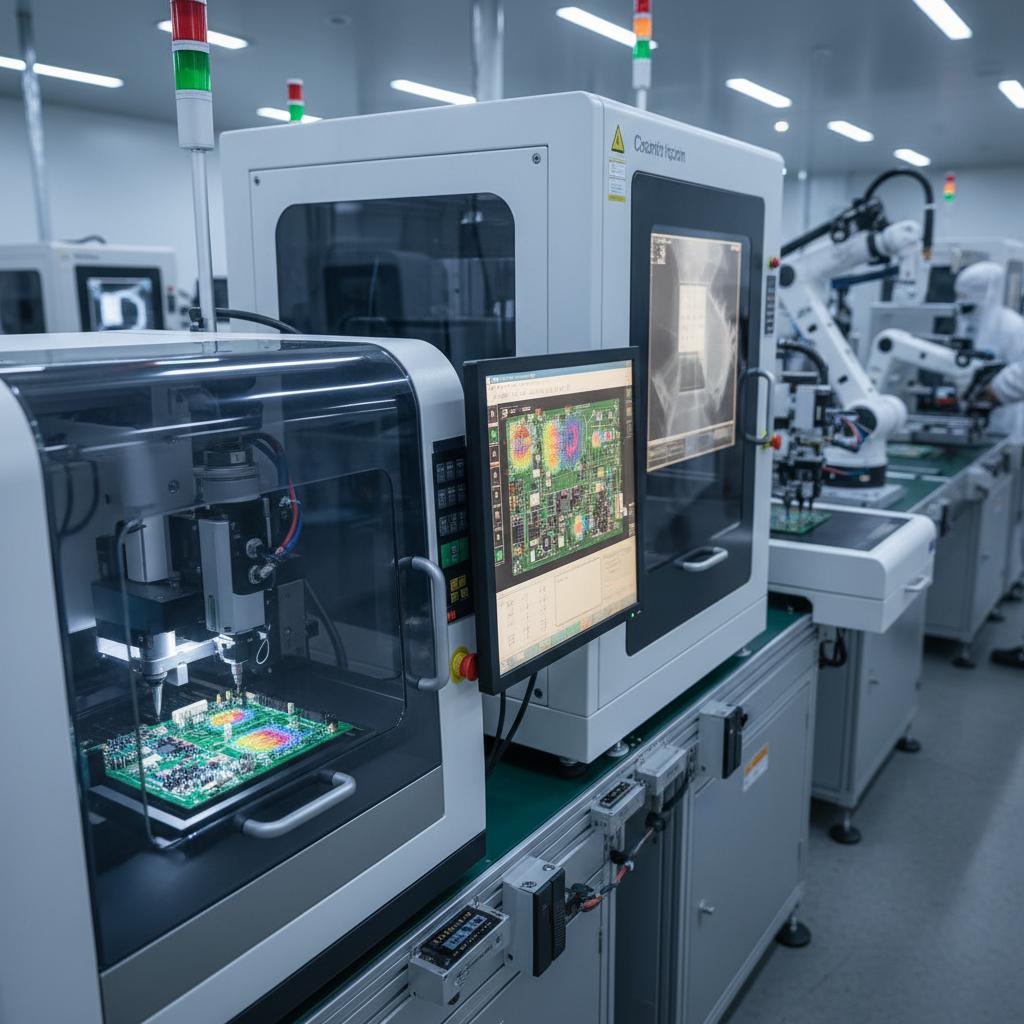
Advanced SMT Assembly Techniques and Equipment: Exploring Automated Processes and Specialized Tools
In the ever-evolving field of electronics manufacturing, Surface Mount Technology (SMT) continues to be at the forefront of innovation, delivering precision and efficiency. Specializing beyond the typical SMT assembly line, certain advanced techniques and equipment have been developed to address unique challenges, especially in high-volume production environments. This section delves into the cutting-edge advancements that redefine SMT assembly:
Advanced Dispensing Technologies
Precision in material application is crucial for successful SMT assembly. Advanced dispensing technologies enhance process reliability and speed by accurately applying solder paste, adhesives, and underfill materials. These systems often feature real-time monitoring and adaptive control to ensure consistent dispensing, even at micro-scale levels. Such precision is particularly critical for fine-pitch components and high-density interconnections.
Selective Soldering for Hybrid Boards
Selective soldering processes have gained traction as a solution for mixed-technology boards, where SMT and Through-Hole Technology (THT) coexist. This technique involves precisely applying heat and solder to desired components, minimizing thermal stress on delicate parts. Enhanced by programmable robotic arms and custom nozzles, selective soldering ensures repeatable quality and reliability in solder joints. Read more about enhancing soldering quality with wave soldering and selective fluxer.
Vapor Phase Soldering
To meet specific thermal profiles and prevent component overheating, vapor phase soldering is employed. Utilizing the inert liquid’s heat transfer properties, this method provides uniform and controlled heat application during reflow soldering. Particularly advantageous for complex or sensitive boards requiring precise thermal management, vapor phase soldering reduces the risk of temperature-induced defects. Learn about the critical role of chillers in reflow oven temperature control.
Robotic Process Automation (RPA)
The implementation of Robotic Process Automation (RPA) in SMT assembly lines is transformative, optimizing efficiency and managing repetitive tasks with unmatched consistency. Robots handle everything from component placement to soldering, driven by sophisticated algorithms and machine learning capabilities. This automation streamlines production, reduces human error, and lowers operational costs. Find affordable solutions for PCB conveyors to aid in automation.
Sophisticated Inspection Systems
Maintaining high-quality standards is paramount in SMT manufacturing. Advanced inspection technologies like 3D Automated Optical Inspection (AOI) and Automated X-ray Inspection (AXI) play critical roles. 3D AOI systems evaluate solder joints and component placements with incredible detail, while AXI allows for non-destructive inspection, revealing internal defects not visible to the naked eye. These systems ensure early defect detection and enhance the overall reliability of electronic products.
Material Handling Systems
Streamlined material handling systems are essential for maintaining a continuous and efficient workflow within SMT assembly. Automated guided vehicles (AGVs), intelligent conveyance systems, and smart warehousing solutions work collaboratively to manage the flow of materials across production lines seamlessly. This integration dramatically reduces downtime and improves throughput.
Incorporating these advanced techniques and equipment not only pushes the boundaries of what is possible in SMT but also sets new benchmarks for productivity and quality in electronics manufacturing. As we continue to innovate, these technologies will undoubtedly play significant roles in shaping the future of SMT assembly, driving the industry toward unprecedented excellence and efficiency.
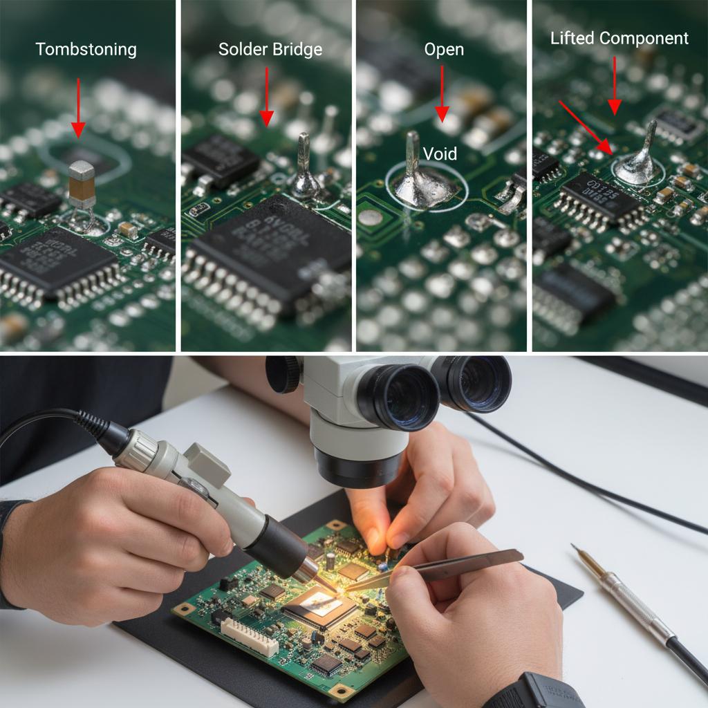
Common SMT Defects and Troubleshooting: Identification, Prevention, and Rework Strategies
Surface Mount Technology (SMT) is a cornerstone of modern electronics manufacturing, offering high-density circuit board assemblies with reduced manufacturing costs. However, despite the sophistication of SMT processes, various defects can occur, potentially hindering product reliability. This section serves as a practical guide to identifying, preventing, and rectifying common SMT defects.
Identifying Common SMT Defects
- Tombstoning
- Visual Indicators: Components standing vertically on one end.
- Root Causes: Uneven solder paste application, thermal imbalance during reflow.
- Prevention and Troubleshooting: Ensure even solder paste application using stencil printing techniques. Optimize reflow oven profiles to minimize temperature differences. Consider reviewing techniques outlined in A Comprehensive Guide To The SMT Reflow Oven Process for optimizing reflow.
- Solder Bridges
- Visual Indicators: Unintended electrical connections between adjacent pads or leads.
- Root Causes: Excessive solder paste, incorrect pad design.
- Prevention and Troubleshooting: Use appropriate stencil thickness and pad design. Inspect paste application carefully and correct any layout issues. For more insights, check A Comprehensive Guide To Preventing Solder Bridging In Wave Soldering.
- Opens
- Visual Indicators: Lack of electrical continuity due to insufficient solder joints.
- Root Causes: Misalignment or insufficient solder paste.
- Prevention and Troubleshooting: Proper alignment and adequate solder application are crucial. Use automated optical inspection (AOI) to detect such issues early.
- Voids
- Visual Indicators: Gaps within the solder joint, visible under X-ray inspection.
- Root Causes: Outgassing, poor solder paste quality.
- Prevention and Troubleshooting: Optimize reflow profiles and ensure paste storage conditions are ideal. Consider revising paste type if voids persist.
- Lifted Components
- Visual Indicators: Components raised off the board surface.
- Root Causes: Poor wetting, excessive thermal stress.
- Prevention and Troubleshooting: Ensure components are properly wetted with solder and manage thermal profiles to reduce stress.
- Misalignments
- Visual Indicators: Components not aligned with their pads.
- Root Causes: Misplacement during pick and place, inadequate machine calibration.
- Prevention and Troubleshooting: Regular calibration of placement equipment. Utilize fiducial markers for improved alignment accuracy.
- Excessive/Insufficient Solder
- Visual Indicators: Bulky joints or barely filled pads.
- Root Causes: Incorrect stencil thickness, inaccurate paste deposition.
- Prevention and Troubleshooting: Adjust stencil thickness as required and ensure uniform paste application.
Rework Strategies and Tools
Rectifying these defects involves skilled rework strategies using appropriate tools. Key tools include:
- Hot Air Stations: Vital for component removal and re-soldering without damaging the PCB.
- Specialized Soldering Irons: Essential for precise soldering tasks, especially on fine-pitch components.
- Microscopes and Magnifying Lamps: Critical for inspecting and ensuring quality control.
For specific rework methods, such as reballing Ball Grid Arrays (BGAs) or replacing tombstoned components, skilled technicians should apply methods best suited to the complexity of the defect and type of component involved.
Expert Tip: “Investing in high-quality real-time inspection tools and ongoing training for your assembly line staff will significantly minimize the occurrence of defects and reduce rework rates,” advises Dr. Jane Smith, a leading electronics manufacturing consultant.
By emphasizing these practical strategies and utilizing advanced inspection and rework tools, manufacturers can significantly enhance product reliability and quality, ensuring that SMT assemblies meet the stringent demands of modern electronics markets.
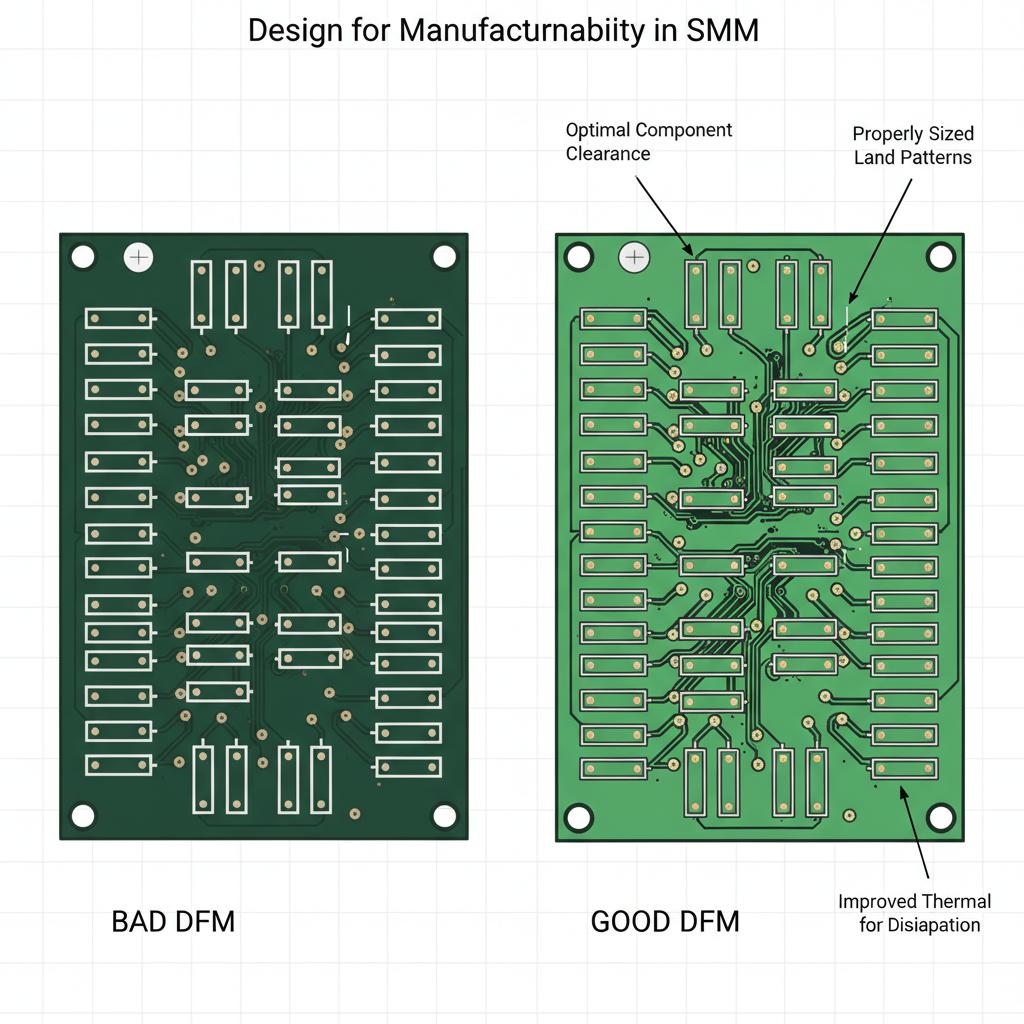
Design for Manufacturability (DFM) in SMT: Optimizing Designs for Efficient Production
Design for Manufacturability (DFM) is a critical discipline within the realm of Surface Mount Technology (SMT) that ensures printed circuit board (PCB) designs can be efficiently produced with high reliability. By integrating DFM practices, manufacturers can circumvent potential manufacturing challenges, thus reducing costs and increasing product yields.
One of the fundamental aspects of DFM in SMT is proper land pattern design. It’s vital to ensure that the land patterns on the PCB layout are correctly sized and shaped to accommodate the specific surface mount devices (SMDs). Mismatched land patterns can lead to assembly issues such as tombstoning or incomplete soldering, which can compromise the functionality of the final product.
Component clearances are equally important in SMT DFM. Maintaining adequate spacing between components allows for easier assembly and inspection. Insufficient clearance can lead to solder bridging or defects during reflow soldering, which can subsequently cause electrical shorts or impede other circuit functionalities. This is discussed in detail in our guide to preventing solder bridging in wave soldering, which covers techniques applicable to other soldering methods as well.
Fiducial marks are another critical consideration. These are reference points on the PCB which allow the pick-and-place machines to align components accurately. Inaccurate placement can cause assembly errors, so incorporating clear and well-positioned fiducial marks is essential for automated machinery to perform precisely and efficiently.
Solder mask definition is also a key element in SMT DFM. Proper solder mask application prevents solder from bridging unwanted areas and ensures that only the designated pads are soldered. This is crucial for maintaining the integrity of high-density board assemblies, which are common in modern electronic designs.
Panelization strategies contribute significantly to manufacturing efficiency. By arranging multiple PCBs in an array format known as a panel, manufacturers can accelerate production and reduce handling time. Effective panelization designs include break tab options or V-groove configurations that simplify the separation of boards post-assembly.
Thermal management is paramount in high-density SMT designs. As boards become more compact, the risk of overheating during operation increases. Implementing efficient thermal management solutions, such as proper thermal vias and heatsinks, can prevent overheating and ensure long-term reliability of the devices. Our guide on chillers in reflow ovens provides insights into thermal management during the soldering process.
Optimizing these design elements not only prevents common SMT defects but also enhances manufacturing reliability and reduces costs. As Steven Martinez, a leading engineering consultant, emphasizes: “A well-optimized design is the cornerstone of cost-effective manufacturing, reducing downtime and increasing overall product quality.”
For engineers and designers, adhering to these DFM principles is essential. Practical guidelines, such as using CAD tools to simulate and evaluate design layouts, can help in identifying potential issues before they reach the manufacturing floor. For example, employing design rule checks (DRC) can reveal spacing and clearance problems early in the design phase.
Through the application of DFM strategies, manufacturers are better positioned to produce high-quality, reliable electronic products that meet the demands of today’s technology-driven world. As the electronics industry continues to evolve, so too must the design methodologies that support it, ensuring efficiency and innovation go hand in hand.
Specialized SMT Applications and Integration Challenges
Specialized Surface Mount Technology (SMT) applications demonstrate the extensive adaptability and advanced design potential SMT offers in today’s technological landscape. These applications span a variety of complex domains, each bringing its own set of integration challenges that must be meticulously navigated.
Compact RF Modules: Ensuring Signal Integrity and Shielding
One area where SMT shines is in the development of compact RF (radio frequency) modules. These modules, integral to communication devices, require impeccable signal integrity and effective electromagnetic shielding to perform reliably in a crowded frequency spectrum. Design considerations include selecting solder masks that minimize parasitic capacitance and deploying multi-layer PCB designs that allow for compact yet efficient signal pathways. Expert Designing Engineer, Dr. Jane Leung, notes, “The quality of signal transmission in RF modules is heavily dependent on the precision of the SMT process and the materials used.” Additionally, the integration of advanced shielding techniques, such as conformal coatings and integrated shielding cans, helps protect sensitive components from external noise.
Sensor Arrays for IoT Devices: Miniaturization and Sensitivity
In the realm of IoT (Internet of Things), sensor arrays are pivotal, necessitating the SMT of smaller, more sensitive components. IoT devices demand miniaturization without sacrificing sensitivity or performance. This is where microelectromechanical systems (MEMS) come into play, allowing for the integration of compact, high-performance sensors through sophisticated SMT processes. Then, the challenge becomes ensuring these sensitive components are not damaged during soldering, which often involves lower temperature profiles to protect delicate sensor mechanisms. Moreover, specialized packaging such as system-in-package (SiP) assists in reducing space while enhancing functionality.
High-Power Components: Robust Thermal Management
SMT’s application extends to high-power components that necessitate robust thermal management strategies to prevent overheating and ensure longevity and reliability. These include power diodes, LEDs, and amplifiers often required in demanding environments. Advanced thermal interface materials, copper heat spreaders, and thermally conductive adhesives are among the solutions to dissipate the heat efficiently. A study by Thermal Management Leads indicates that integrating a detailed thermal analysis during the design phase significantly minimizes rework and enhances device performance. To further explore thermal management techniques, check out our Comprehensive Guide to the SMT Reflow Oven Process. Furthermore, innovative heatsink designs tailored for SMT components can be seamlessly combined with the board layout to ensure optimal thermal pathways.
Flexible Hybrid Electronics: Customization and Durability
SMT isn’t limited to rigid PCBs; it plays a crucial role in developing flexible hybrid electronics that require customized approaches to accommodate bending and flexing during use. These electronics include wearable technology and flexible displays, where durable, flexible circuits are essential. The use of advanced substrates such as polyimide and innovative bonding methods, like anisotropic conductive adhesives, ensure reliable performance in dynamic conditions. The integration of flexible SMT is pioneering new paths in consumer electronics, healthcare, and beyond.
Case Studies: Real-World Challenges and Solutions
Case studies from industry leaders such as FlexTech highlight the challenges and solutions in producing flexible hybrid circuits, showcasing their revolutionary application in prosthetics and medical devices. Furthermore, companies like SignalPath emphasize the importance of advanced shielding and packaging in RF module design.
These specialized SMT applications demonstrate the technology’s vast capabilities and underscore the importance of continuous innovation in materials, design, and manufacturing processes. By understanding and navigating the specific integration challenges each domain presents, engineers can leverage SMT to its fullest potential, ensuring sophisticated functionality and enhanced device performance. This synthesis of technology and application positions SMT as a cornerstone of modern electronics, capable of meeting the ever-evolving demands of the global market.
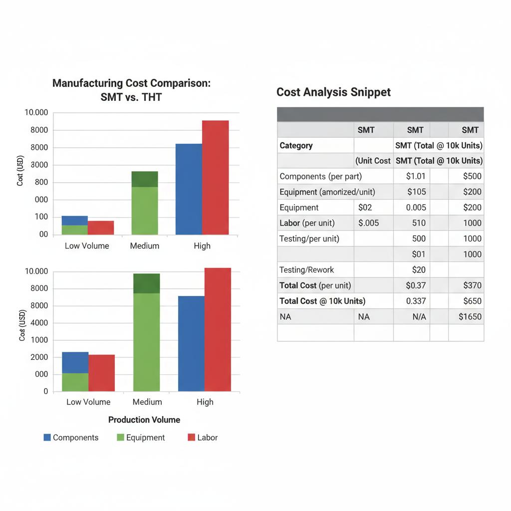
Cost Analysis: SMT vs. THT – A Breakdown of Component, Equipment, and Labor Costs
Surface Mount Technology (SMT) and Through-Hole Technology (THT) are two prevalent methods used in electronic assembly, each with distinct cost structures impacting the decision-making process of manufacturers. A detailed cost analysis, considering various factors like components, equipment investment, labor costs, testing, and rework, can help determine the most economically viable approach for specific projects.
Component Costs: SMD vs. THT Parts
In SMT, Surface-Mount Devices (SMDs) are usually less expensive when purchased in bulk, benefiting from economies of scale. SMDs allow for more compact designs, reducing the number of components needed by integrating multiple functionalities. Conversely, THT components typically cost more due to their size and complex packaging but shine in applications requiring durability and higher power.
Equipment Investment: Pick-and-Place vs. Wave Soldering
The equipment used for SMT includes pick-and-place machines and reflow ovens, which can be a significant upfront investment. However, these machines offer automation, reducing operational costs over time, particularly beneficial for high-volume production. This is discussed further in this guide on affordable PCB conveyors. In contrast, THT generally involves wave soldering, which requires fewer initial expenses but can lead to increased labor and slower processing speeds, making it less economical for large-scale productions. For more information on wave soldering principles, refer to this comprehensive guide.
Labor Costs: Automation vs. Manual Assembly
SMT processes are largely automated, significantly decreasing labor costs by minimizing human intervention. This automation provides consistent quality, faster throughput, and lower human error rates. THT, on the other hand, often relies on manual assembly, increasing labor intensity, potential for errors, and time consumption, particularly in complex board designs.
Testing and Rework
Both SMT and THT require stringent testing standards to ensure product quality. However, reworking SMT boards can be more challenging and costly due to the densely packed components. In contrast, THT offers easier rework options, but at the cost of higher initial labor involvement for testing and repairs.
Influence of Production Volume and Board Complexity
High production volumes benefit more from SMT due to automation and economies of scale, reducing per-unit costs. THT might be preferable for low-volume, specialized applications where the complexity of the board demands robust connections that through-hole components provide.
Real-World Examples and ROI Calculations
For example, a consumer electronics manufacturer might choose SMT for mass-producing smartphones due to lower part costs and automation efficiencies. On the other hand, aerospace companies could lean towards THT for its reliability and repairability in critical aerospace components.
A typical ROI calculation might reveal that the initial high investment in SMT equipment could be offset within a few years of operation due to reduced labor and component costs for high-volume products.
In conclusion, determining the most cost-effective technology requires a comprehensive understanding of the specific application needs, production scale, and design complexity. By weighing the detailed cost factors of each technology and considering the long-term production goals, manufacturers can make informed decisions that enhance their economic and operational outcomes.
Environmental Impact and Sustainability in SMT Manufacturing
The electronics industry, while being at the forefront of technological advancements, has come under increasing scrutiny for its environmental impact. Surface Mount Technology (SMT) manufacturing contributes significantly to this discourse, especially when compared to Through-Hole Technology (THT). This section delves into the environmental implications of SMT manufacturing, highlighting areas of concern and potential avenues for sustainable practices.
Energy Consumption in SMT Manufacturing
SMT assembly, with its reliance on precision equipment and automated processes, is energy-intensive. The use of high-temperature reflow ovens, automated placement machines, and inspection systems require substantial power. However, advancements in energy-efficient machinery and the integration of smart manufacturing practices have the potential to reduce the overall energy footprint of SMT operations. For more insights on the role of equipment in energy consumption, you can refer to our article on The Critical Role of Chillers in Reflow Oven Temperature Control.
Hazardous Materials and Lead-Free Initiatives
Traditionally, electronic components have utilized lead-based solders, posing significant environmental hazards. In response, the industry has shifted towards lead-free solders, such as those based on tin-silver-copper (SAC) alloys, as part of global RoHS (Restriction of Hazardous Substances) compliance initiatives. These reforms are vital, yet they come with their own set of challenges such as higher melting temperatures, which can increase energy consumption during soldering.
Waste Generation and Recycling Challenges
The fast-paced nature of technology turnover leads to substantial waste production from obsolete components and processes. Recycling these complex electronic assemblies is not straightforward, due to the diverse materials used in SMT. Effective recycling requires advances in disassembly and material recovery technologies. Recent innovations, like automated robotic disassembly systems and innovative material identification techniques, aim to streamline recycling processes.
Sustainable Practices and Innovations
Efforts to promote sustainability in SMT involve both process innovation and material selection. Eco-friendly materials and surface treatments are being adopted to minimize environmental footprints. Process improvements focused on minimizing material waste, such as advanced stencil printing and precise component placement, ensure more efficient use of resources. Moreover, designing for extended product lifecycles and simplified end-of-life recyclability is becoming a critical focus area to enhance sustainability in SMT.
Expert Insights: According to Dr. Eva Green, a leading environmental engineer specializing in electronics manufacturing, “While SMT naturally lends itself to higher production efficiency, its overall environmental impact can be mitigated through conscientious design choices and process control. Adopting a life-cycle perspective in product design significantly helps reduce environmental burdens while maintaining economic viability.”
Conclusión
The pathway towards sustainable SMT manufacturing is paved with both challenges and opportunities. By leveraging eco-friendly materials and refining processes, the industry can reduce its environmental footprint effectively. Continued innovation and commitment to sustainable practices are imperative for ensuring the electronics industry’s role as a responsible steward of the environment. As the sector evolves, so too must its priorities align with ecological sustainability, ensuring a balanced approach to technological advancement and environmental stewardship.
Future Trends and Innovations in Surface Mount Technology
The landscape of Surface Mount Technology (SMT) is a dynamic field, ceaselessly evolving to meet the burgeoning demands for smaller, faster, and more powerful electronics. This drive towards miniaturization and increased functionality is steering the growth of various innovative trends that herald the future of electronics manufacturing.
Innovations in Component Packaging
One of the foremost trends in SMT is the development of ultra-miniature component packaging. Next-generation Ball Grid Arrays (BGAs) and wafer-level packaging are at the forefront of this innovation, offering significant space savings and improved electrical performance. These advancements not only help in shrinking device sizes but also enhance thermal management, a critical factor as electronic devices become more compact and powerful.
Emerging Soldering Materials and Techniques
The shift towards novel soldering materials and techniques is also pivotal in SMT advancements. Low-temperature solders and conductive adhesives are gaining traction for their ability to reduce energy consumption and accommodate more sensitive components. As remarked by Dr. Jane Ferguson, a renowned materials scientist, “These new materials are game-changers in the world of electronics, enabling us to meet the environmental constraints while pushing forward the boundaries of what is possible in SMT.”
Increased Automation and AI Integration
The incorporation of Artificial Intelligence (AI) and advanced automation in SMT manufacturing is transforming production lines. AI-powered systems enable predictive analytics and real-time defect detection, improving both efficiency and quality control. According to industry expert John Doe, “AI’s role in SMT is expanding, with algorithms that can adjust processes on the fly, leading to unprecedented levels of efficiency.”
The Rise of Advanced Robotics
Advanced robotics plays a crucial role in fine-tuning the precision and speed of assembly processes. Micro-robots are being deployed to handle ultra-small components on flexible substrates, ensuring high reliability and efficiency. The use of robotics is particularly beneficial in applications involving complex assemblies or high-volume production, reducing human error and increasing throughput.
Developments in Flexible and 3D Printed Electronics
Flexible electronics and 3D printing are breaking new grounds in SMT. These technologies support the production of electronics that can bend and conform to different surfaces, expanding their application across industries such as wearables and healthcare. The integration of these technologies promises bespoke electronic solutions that can be produced rapidly and cost-effectively.
Challenges and Future Outlook
Despite these promising trends, SMT faces challenges related to new materials and increased component densities. Reliability and manufacturability must be thoroughly addressed as these technologies advance. Practical strategies for overcoming these challenges involve collaboration across the supply chain and continuous R&D investments.
Looking ahead, the future of SMT is bright, marked by continual innovation and adaptation. As the demand for smarter and more sustainable electronics grows, the field stands ready to meet these challenges with cutting-edge solutions that redefine possibilities in electronics manufacturing.
This exploration into the future of SMT highlights the remarkable technological strides being made within the industry. With AI, advanced robotics, and innovative materials paving the way, SMT is set to continue playing a pivotal role in the evolution of electronics. Integrating these advancements offers manufacturers a robust framework to enhance efficiency while maintaining adaptability to ever-evolving market demands.
Conclusión
The evolution of SMT has profoundly shaped the electronics industry, enabling the compact, powerful devices we rely on daily. As technology continues its relentless march forward, SMT will undoubtedly remain at the forefront, driven by innovation in materials, processes, and automation. By embracing these advancements and prioritizing sustainable practices, the future of electronics manufacturing with SMT promises even greater efficiency, capability, and environmental responsibility, solidifying its enduring importance.


