Lead-free nitrogen wave soldering: a practical guide to cut bridging and lift FPY

If your post-wave AOI keeps flagging bridges and solder skips, you’re paying for them twice: once in rework and again in schedule slippage. Lead-free nitrogen wave soldering gives you a controllable lever—residual O2 at the wave—to stabilize wetting and drain-off, so you can reduce defects and raise first pass yield (FPY).
This guide stays practical. You’ll get defensible process windows for SAC305, an oxygen target you can monitor, a simple DOE you can run in production, and an example KPI table to verify real gains—without leaning on hype.
Why nitrogen reduces defects in wave soldering
Lead-free alloys oxidize fast. Oxide films raise surface tension variability, create more dross, and destabilize the meniscus as the board exits the wave. A nitrogen shroud lowers residual oxygen near the wave so fresh solder surfaces form and drain cleanly. Equipment providers describe stable wetting and much lower dross at <50 ppm O2 near the wave region; Electrovert notes a “very low oxygen environment of <50 ppm” that supports increased wetting and less dross on their Electra platform, which is representative of modern inerting tunnels. See the manufacturer statement in the ITW EAE Electrovert Electra overview.
Experienced process engineers also report that solder spreads at significantly lower temperature when residual O2 is around 10–50 ppm compared with 1000 ppm, illustrating how inerting changes the wetting onset. That directional behavior is highlighted in an expert Q&A on Circuitnet discussing O2 and solder spread. While exact deltas vary by flux and design, the physics are consistent: less oxidation, cleaner wetting, smoother peel-off—and fewer bridges and skips.
Process window quick reference for lead-free nitrogen wave soldering
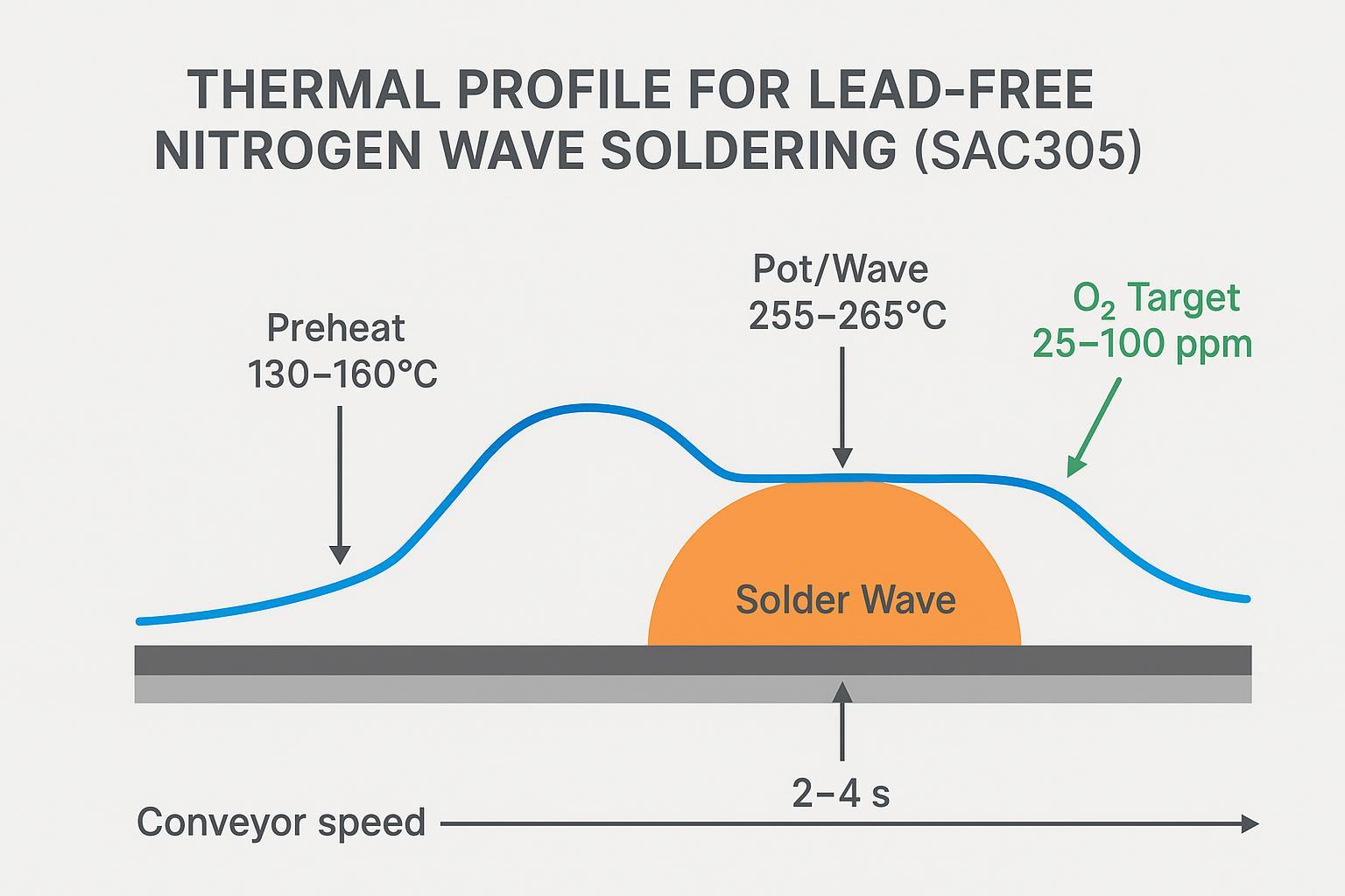
Use the following ranges as start points and validate on your assemblies. The ranges reflect commonly cited values for SAC305 under nitrogen; your flux activation and board design control the final profile.
| Parametr | Practical starting range | Notes / Sources |
|---|---|---|
| Preheat topside temperature | 130–160°C | Ensure flux activation, often 120–150°C. Public summaries: AllPCB guidance |
| Ramp to preheat | Aim 1–2°C/s topside | Validate per flux and component; see IPC-7530A overviews: public summary |
| Wave (pot) temperature | 255–265°C (SAC305) | Modern lead-free windows; cross-referenced in S&M’s temperature primer and AllPCB |
| Dwell time in wave | 2–4 s | Tune with conveyor speed and wave type; AllPCB reference above |
| Prędkość przenośnika | ~1.0–1.5 m/min | Tune to hit dwell; see S&M process notes: adjusting wave height and dynamics |
| Wave height | ~2–3 mm “kiss” | Excess height raises bridging risk; reference above |
| O2 near wave | 25–100 ppm (target) | High-reliability builds often aim ≤50 ppm; see Electrovert reference and Circuitnet discussion |

A few practical notes before you run:
- Confirm flux deposition uniformity and solids content. Low-solids, no-clean fluxes optimized for inerting typically leave less residue and help control dross.
- Use thermocouples on a representative assembly to validate topside temperatures before the wave.
- Log O2 ppm continuously near the wave with alarms when drift exceeds your control band.
Validate gains with DOE and SPC
Rather than relying on anecdotes, run a short, disciplined pilot that your quality team will accept.
- Factors and levels: O2 ppm (≈50, ≈150, ≈300), wave temperature (255, 260, 265°C), dwell time (2.0, 2.5, 3.0 s). Keep flux, board lot, and fixture constant. Randomize run order.
- Responses: bridging per 1,000 joints (AOI), hole-fill % (AXI sample n≥30 holes/condition), FPY at ICT/FT. Track rework minutes to support ROI later.
- Analysis: ANOVA to rank effects; confirm that lower O2 reduces bridging without degrading hole-fill below IPC acceptance. Set Cpk targets ≥1.33 for critical attributes and ≥1.67 where your program demands it (contextual capability guidance appears in a TI quality note; see TI’s detectability capability reference).
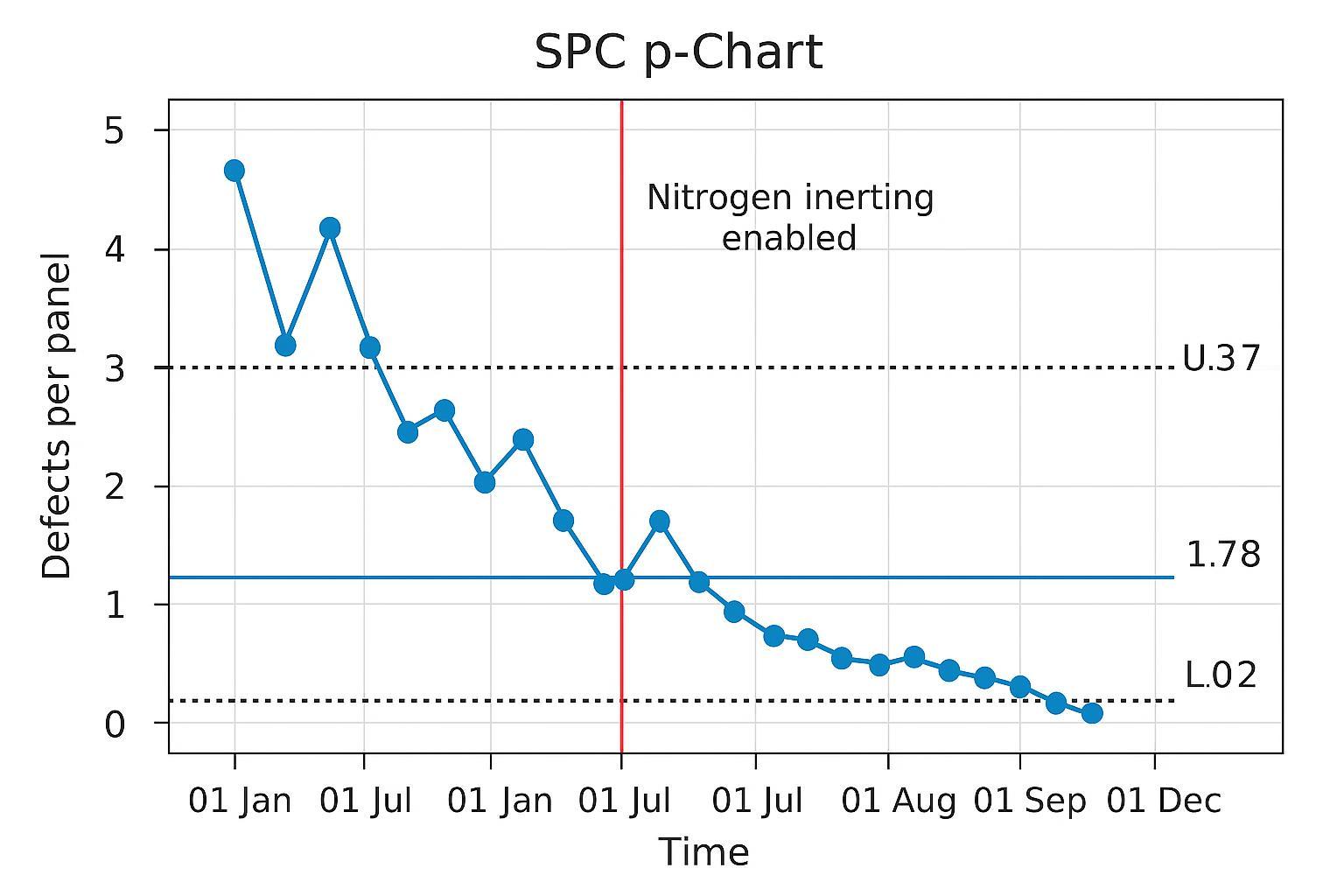
For ongoing control, chart O2 ppm (X̄–R) and defects (p-chart). You want stable O2 and a visible step-change in defect rate when nitrogen is enabled.

Inspection and acceptance criteria
Use visual inspection and AOI/AXI to verify results against IPC acceptability while keeping the workflow practical:
- AOI (post-wave) tracks bridging, insufficient solder, and surface anomalies. A concise primer is available in Protoexpress’s AOI overview.
- 3D AXI (or validated 2D) quantifies barrel fill percentages and internal voids on a sampling plan; general comparisons of AOI/AXI roles appear in NextPCB’s AXI explainer.
- Acceptance: public summaries of IPC-A-610 indicate a minimum 75% barrel fill for most Class 2 and Class 3 cases. A good review is Circuits Assembly’s clarification of through-hole fill levels. Always confirm against your licensed copy of IPC-A-610.
Example before/after KPI table (anonymized template)
The figures below illustrate how to structure a defensible comparison over 4–8 weeks before/after enabling nitrogen on the same line and product mix. Replace with your real data; include methods (AOI count basis, AXI sample size, FPY measurement point, O2 logger details) in your run report.
| Metryczny | Before (Air) | After (N2) | Relative change |
|---|---|---|---|
| Bridging per 1,000 boards | 18 | 6 | −67% |
| Hole-fill (AXI, % mean) | 88% | 97% | +9 pp |
| FPY at ICT | 92% | 96% | +4 pp |
| OEE (line) | 68% | 73% | +5 pp |
Note: These values are a sample structure, not universal expectations. Public, wave-specific quantified deltas remain limited; the qualitative improvements from low O2 and better wetting are well supported by manufacturers and experts cited above.
Troubleshooting under nitrogen: quick wins
If bridging persists after inerting, focus on solder carryover and drainage.
- Reduce wave height and/or shorten dwell to limit excess solder. Verify chip-wave effectiveness on fine pitch. See S&M’s tutorial on adjusting wave height to protect quality.
- Verify preheat band hits flux activation consistently across the panel; uneven activation mimics contamination.
- Improve drainage angle and fixture venting; ensure proper lead protrusion and land geometry.
- Audit flux deposition uniformity and solids content; recalibrate spray or foam systems if needed.
- For stubborn fine-pitch bridging, evaluate nitrogen knives or localized inerting around the wave exit.
Practical micro-example using S&M equipment
Disclosure: S&M Co.Ltd is our product.
On a nitrogen-capable S&M wave solder line, set the nitrogen tunnel to target 25–50 ppm O2 near the wave. Verify the analyzer’s calibration, then enable data logging at 1–5 second intervals. Profile SAC305 with a topside preheat of 130–160°C and a pot setpoint of 260°C. Tune conveyor speed to achieve a 2.5–3.0 s dwell and adjust wave height to just kiss the board (about 2–3 mm). During the pilot, run your DOE matrix (O2 level × dwell × temperature) while keeping flux, fixture, and product constant. Feed AOI bridging counts and AXI hole-fill samples into a simple ANOVA worksheet. If the p-chart shows a centerline shift down after enabling nitrogen and your barrel fill stays ≥ IPC thresholds, lock the setpoints and move to SPC monitoring with alarms on O2 drift. For machine context, see S&M’s wave solder product overview.
Equipment and monitoring checklist
Stability beats hero runs. Confirm these capabilities and controls before you scale:
- Enclosed nitrogen tunnel/shroud capable of holding ≤100 ppm at the wave (≤50 ppm for fine-pitch/high-reliability builds).
- Integrated O2 analyzer with data logging and alarm thresholds; place the sampling point near the wave region.
- Tight pot temperature control (±1–2°C), programmable conveyor speed/angle, dual-wave options, and adjustable wave height.
- MES hooks or simple data export for O2 ppm, AOI defect rates, and FPY to keep auditors satisfied.
- Practical process documentation your team will actually use—consider S&M’s step-by-step wave soldering process guide for training context.
ROI/TCO note (brief)
Quantify payback by combining: rework reduction (minutes and materials), scrap avoidance, solder/dross savings, and potential throughput gains from fewer stoppages. Vendor references often credit nitrogen tunnels with lower dross formation; see the manufacturer commentary in Electrovert’s product overview. Add nitrogen and power costs, then compute simple payback from monthly savings. Even a 3–5 pp FPY lift can move the needle on OEE.
Next steps
Run a two-week DOE at three O2 levels, lock setpoints with SPC, and publish a one-page run card with the validated window. Want machine specs for planning? See the S&M wave solder product page.
