You can solve solder bridging in wave soldering by acting fast and using proven repair methods. Quick identification and action keep your yield high and costs low. For example, automatic optical inspection (AOI) detects 99.5% of defects, boosting yield rates by up to 20% and cutting rework costs by 40%. Many defects come from poor fixture design, with aperture size errors causing 42% of bridging cases. Addressing these root causes helps you reduce defects and improve your production process.
Key Takeaways
-
Act quickly to fix solder bridging. Use a soldering iron with solder wick or sucker to remove excess solder and keep production moving.
-
Regularly inspect your work. Use visual checks and electrical testing with a multimeter to ensure repairs are solid and prevent future issues.
-
Optimize your soldering process. Adjust wave height, flux application, and preheating to reduce the risk of solder bridging.
-
Design PCBs carefully. Maintain proper spacing between pads and use solder mask dams to prevent unwanted connections.
-
Utilize automated inspection methods. Automated Optical Inspection (AOI) and X-ray systems help catch defects early, saving time and costs.
Fixing Solder Bridging

Quick Production Fixes
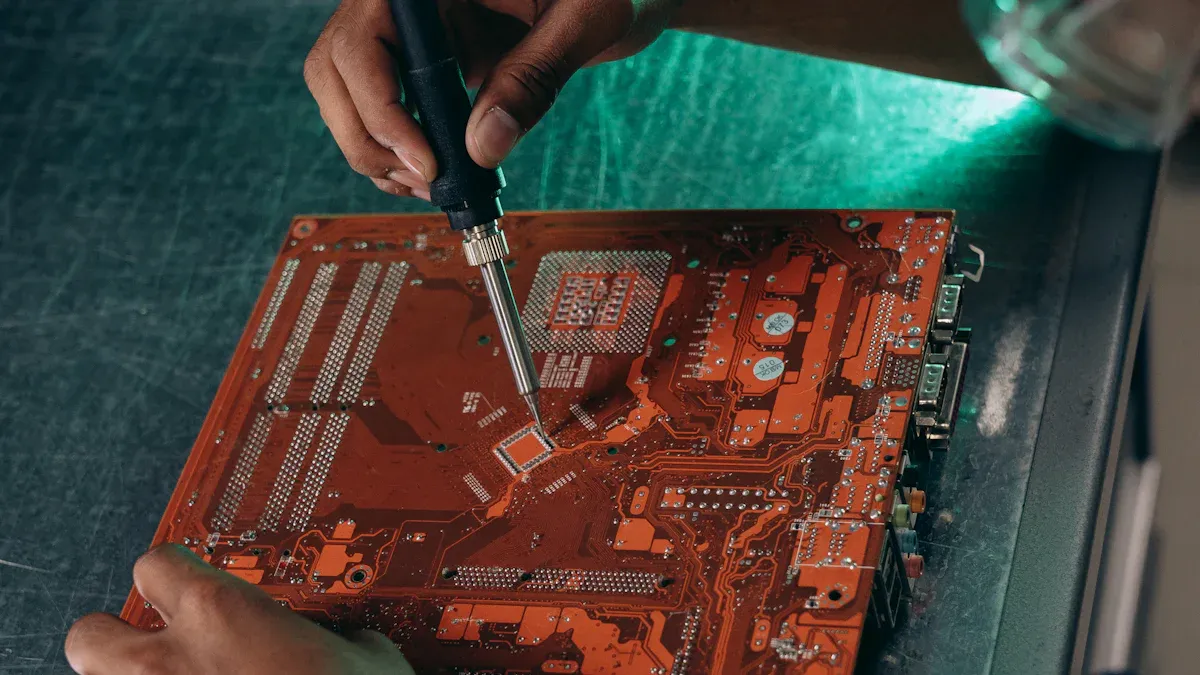
When you spot solder bridging during wave soldering, you need to act fast to keep your production line moving. Start by identifying the affected area. Use a soldering iron to heat the bridge, then choose the right tool to remove excess solder.
|
Pros |
Cons |
|
|---|---|---|
|
Solder Wick |
Precise, ideal for small areas, works well for SMT components |
Time-consuming for large amounts, may leave residue |
|
Solder Sucker |
Faster for larger bridges, handles bigger volumes |
Requires skill to avoid damage, less effective in tight spaces |
You can use solder wick for small, tight spots. Place the wick over the bridge, apply the iron, and let the solder soak into the braid. For larger bridges, a solder sucker works well. Heat the solder, trigger the sucker, and pull away the excess. Always check your work to avoid damaging pads or traces.
You can also make quick process adjustments to prevent further solder bridging:
-
Lower the wave height if you see too much solder collecting on leads.
-
Adjust the flux application to ensure even coverage and reduce bridging.
-
Apply a protective coating to stop solder from forming unwanted connections.
Tip: Keep your tools clean and well-maintained. Dirty tips or clogged suckers can make repairs harder and less effective.
Post-Soldering Actions
After you remove a solder bridge, you need to make sure the repair is solid. Visual inspection helps, but electrical testing gives you real confidence. Use a multimeter to check the repaired area.
-
Set your multimeter to continuity mode.
-
Touch the probes to the pads or leads that were bridged.
-
Listen for a beep or check the display for low resistance. This means you have a good connection.
-
Test nearby pads to confirm you did not create a new bridge.
A multimeter helps you find hidden problems. It ensures the circuit works as designed and that all components are properly soldered. Electrical connection tests are vital in PCB manufacturing. They help you catch issues before the board moves to the next stage.
Note: Always test after every repair. This step prevents costly rework and keeps your quality high.
By following these steps, you can fix solder bridging quickly and keep your production line running smoothly.
Solder Bridging Causes
Common Process Issues
You can prevent many soldering problems by understanding what causes them. Solder bridging often starts with process mistakes during wave soldering. The table below shows some of the most common process-related issues and their effects:
|
Cause |
Description |
|---|---|
|
Too much flux can lead to bridging. |
|
|
Inadequate flux coverage |
Not enough flux can cause drainage issues. |
|
Inadequate solder pot temperature |
Incorrect temperature affects soldering quality. |
|
Board immersion depth |
Immersing too deeply can lead to bridging. |
|
Improper solder pot maintenance |
Dross can affect solder quality. |
|
Poor component solderability |
Oxidation or poor plating can hinder soldering. |
You might also see problems if you use fast conveyor speeds or set preheating temperatures too low. These mistakes can lower solder viscosity and make bridging more likely. Poor PCB design, such as narrow pad pitches or irregular pin placements, can also create process challenges.
Tip: Regularly check your solder pot and flux application to catch these issues early.
Design-Related Factors
Your PCB design choices play a big role in preventing solder bridging. If you place pads or traces too close together, you increase the risk of bridges, especially when pad spacing drops below 0.2 mm. Missing solder mask between pads exposes more copper, which can also cause unwanted connections.
To reduce the risk, follow these design tips:
-
Align through-hole components parallel to the solder wave direction to avoid shadowing.
-
Keep at least 2.54 mm (0.1 inches) between through-hole leads.
-
Place taller components at the trailing edge of the wave to prevent shadowing.
-
Group similar components together for even soldering.
-
Use via tenting to cover exposed annular rings and minimize shorts.
-
Maintain a minimum solder mask web of 4 mil for green and 5 mil for other colors.
-
Match the solder mask opening to the pad size to avoid extra copper exposure.
Careful planning and smart design choices help you avoid solder bridging and improve your overall yield.
Identifying Solder Bridging

Visual Inspection
You can spot solder bridging early by using careful visual inspection. Start by examining the solder joints under good lighting. Use a magnifying glass or a microscope with at least 10x magnification. Look for shiny, continuous solder connections between pins or pads that should not be connected. These bridges often appear as small blobs or lines of solder joining two points.
The simplest way to spot solder bridges is through careful visual inspection under magnification. Using a microscope with at least 10x magnification, look for shiny, continuous solder connections between adjacent pads or pins that shouldn’t be connected.
In large-scale manufacturing, you often rely on Automated Optical Inspection (AOI) systems. AOI uses high-resolution cameras and smart algorithms to scan each PCB for defects. This method can detect solder bridging with up to 99.9% accuracy. AOI systems catch problems early, so you can fix them before the boards move further down the line.
You may also use Automated X-ray Inspection (AXI) for more complex boards. AXI helps you find hidden bridges that visual checks might miss, especially under large components.
-
Visual Inspection: Examine solder joints under magnification for defects.
-
AOI: Use cameras and software to detect bridges quickly and accurately.
-
AXI: Apply X-ray imaging to spot hidden solder issues.
Electrical Testing
After you finish visual checks, you should confirm your results with electrical testing. This step helps you find any hidden solder bridging that you might have missed.
|
Description |
|
|---|---|
|
Continuity Testing |
Checks for shorts between pins or pads using a multimeter. A beep or low resistance indicates a solder bridge. |
|
Power-on Testing |
Involves powering the circuit to observe unusual behavior, which may indicate solder bridges. |
Set your multimeter to continuity mode. Touch the probes to the pins or pads in question. If you hear a beep or see low resistance, you have found a bridge. Power-on testing can also reveal problems. If the board behaves strangely or does not work, check for solder bridging again.
Preventing Solder Bridging
Process Adjustments
You can prevent most solder bridging issues by making targeted process adjustments. Start by optimizing how you align components and manage the soldering process. Proper alignment keeps solder from skipping pads or forming uneven joints. Adjusting SMD footprints and adding dummy thieving pads to high-pin-count connectors also helps. These changes improve yield and reduce the chance of bridges.
|
Process Adjustment |
Description |
|---|---|
|
Prevents solder skips, uneven fillets, and bridges. |
|
|
Modifying SMD footprints |
Ensures proper gaps and adds solder thieving for better yield. |
|
Using dummy thieving pads |
Pulls excess solder away from trailing pins on large connectors. |
|
Controlling board-wave interaction |
Manages dwell time and immersion depth to reduce defects. |
You should also control solder wave height and volume. Keep the wave height between 8–12 mm for best results. If the wave is too low, you get incomplete coverage. If it is too high, you risk splatters and bridging. Avoid excessive pump pressure, which can create unstable waves and increase defects. Set the wave height to no more than 50% of the PCB thickness relative to the pallet. This prevents component lifting and extra solder from forming bridges.
Adjust conveyor speed and solder temperature for optimal results. A conveyor speed of 1000 mm/min and a solder temperature above 230°C can lower bridging defect rates to less than 0.3%. These settings help you achieve full pad coverage without causing voids or excess solder.
Tip: Regularly check your process parameters. Small changes in speed, temperature, or wave height can have a big impact on solder quality.
Flux and Preheating
Choosing and applying flux correctly is essential for preventing solder bridging. Select a flux that matches your PCB and component materials. Apply it evenly using a spray or foam system. Uniform coverage ensures that solder flows only where you want it.
The temperature and activity of your flux matter. If the flux gets too hot during formulation, its viscosity drops. This can make solder more likely to bridge. Preheating the PCB before wave soldering improves solder flow and pad wetting. A steady, controlled preheat helps the flux work properly and reduces the risk of bridging. Avoid heating the board too quickly, as this can cause the flux solvent to evaporate too fast, leading to poor wetting and uneven joints.
-
Preheat the PCB to enhance solder flow and achieve uniform joints.
-
Maintain the right preheat temperature and dwell time so the flux does not burn off before soldering.
-
Match flux activity to the solderability of your components to avoid over-activation.
-
Monitor humidity and temperature in your work area for consistent flux performance.
Note: Larger pin count connectors should be oriented perpendicular to the wave. If you cannot change the orientation, use solder thieves to pull excess solder away from trailing pins. Angling the PCB between 15–30° in the solder pallet also helps reduce bridging.
Solder Mask and PCB Design
Good PCB design plays a major role in preventing solder bridging. Use solder mask dams between pads to create barriers that keep solder from flowing where it should not go. Solder masks prevent bridges by blocking solder from connecting adjacent pads. Apply the solder mask carefully, especially between component pins.
Add copper solder thieves near closely spaced pads. These features pull excess solder away from critical areas, reducing the risk of bridges. Make sure your pad and hole sizes are correct. Oversized pads decrease the distance between pins and increase the chance of bridging. Maintain proper spacing between components and use fiducial marks to help with accurate placement.
-
Solder mask dams act as barriers to contain solder.
-
Copper solder thieves redirect excess solder away from sensitive areas.
-
Proper pad sizing and spacing reduce the risk of unwanted connections.
Alert: Improper pad spacing, especially less than 2.54 mm, greatly increases the risk of solder bridging.
Inspection and Feedback
Regular inspection and feedback help you catch solder bridging early and improve your process over time. Use a mix of manual and automated inspection methods. Visual inspection with magnification tools lets you spot obvious defects. Automated Optical Inspection (AOI) systems use cameras and software to detect bridges quickly and accurately. AOI can reduce false negatives by up to 90% and inspect a full PCB in under 10 seconds. X-ray inspection finds hidden bridges that you cannot see from the outside.
|
Inspection Method |
Description |
|---|---|
|
Visual Inspection |
Manual process using magnification to find solder bridges. |
|
Automated Optical Inspection (AOI) |
Uses cameras and software for fast, accurate defect detection. |
|
X-ray Inspection |
Finds hidden defects like voids and bridges not visible externally. |
Inspection also acts as a feedback mechanism. By monitoring defect rates and conducting regular audits, you can spot trends and make process improvements. Statistical process control (SPC) helps you identify variations and refine your soldering process. Early detection and feedback save you money by reducing rework and preventing recalls.
-
AOI systems catch small defects before they become big problems.
-
Regular audits and SPC help you maintain high quality.
-
Inspection feedback lets you adjust upstream processes for better results.
Tip: Use inspection data to drive continuous improvement. The more you learn from defects, the fewer you will see in the future.
You can solve solder bridging in wave soldering by following a few key steps. Always check your waveform, confirm soldering coordinates, and ensure proper flux loading. Adjust preheat temperature and soldering time as needed. Ongoing process monitoring, like using Statistical Process Control or yield trend analysis, helps you catch issues early.
-
Attend hands-on training programs such as Science of Soldering© or CTTI classes.
-
Keep your process simple and maintain clearances in your designs.
-
Regular testing and feedback improve product reliability and reduce costly rework.
Consistent prevention and training boost your yield and strengthen your brand reputation.
FAQ
What is solder bridging in wave soldering?
Solder bridging happens when solder connects two or more pads or pins that should stay separate. This creates an unwanted electrical connection. You can spot these bridges as shiny lines or blobs between pins.
How can you quickly fix a solder bridge?
You can use a solder wick or a solder sucker to remove the excess solder. Heat the bridge with a soldering iron, then apply your chosen tool. Always check your repair with a multimeter.
What causes most solder bridging defects?
Most solder bridging comes from too much solder, poor flux application, or incorrect PCB design. You might also see bridging if you set the wave height or temperature wrong.
How do you prevent solder bridging before it starts?
You should optimize your process. Adjust wave height, flux, and preheat settings. Use solder mask dams and keep enough space between pads. Regular inspection helps you catch problems early.
Can you use automated inspection to find solder bridges?
Yes, you can use Automated Optical Inspection (AOI) or X-ray systems. AOI finds the most visible bridges fast. X-ray inspection helps you spot hidden bridges under large components.
