
Published: 09 July 2026
Last Updated: 09 July 2026
Reading Time: 13 minutes
Reviewer: [Reviewer name placeholder – not provided]
Author: Jace Liu
—> Published: 09 July 2026
Last Updated: 09 July 2026
Reading Time: 13 minutes
Reviewer: [Reviewer name placeholder – not provided]
Author: Jace Liu
Why Reflow Soldering Defects Still Matter in 2026
Here’s a number that keeps SMT managers up at night: solder joint defects account for about 60% of all SMT-related failures in electronics manufacturing [1]. That’s not some small problem hiding in a corner. It’s the big thing sitting right in the middle of your production floor.
I remember visiting a smartphone assembly line where tombstoning was running at about 2% on QFN components. Sounds small, right? But when you’re pushing 50,000 units a day, that adds up to thousands of failed boards every single day. The rework station became the bottleneck, and engineers scrambled for weeks trying to get things under control.
This article breaks down the reflow soldering defects you need to know about. Common issues include bridging, tombstoning, voids, solder balls, beading, wetting problems, insufficient solder, cold joints, head-in-pillow (HiP), opens, and component shift. But here’s the thing: these aren’t just cosmetic problems that look bad under magnification. They can hurt electrical performance, reduce mechanical strength, tank thermal reliability, and cut short the lifespan of products in the field.
For automotive and aerospace manufacturers, these defects aren’t just expensive. They can be dangerous.
The good news? High-volume SMT lines with closed-loop process control see 60-80% reductions in rework and scrap [1]. Getting smart about what causes these defects is the first step toward stopping them, and that’s exactly what we’ll cover in this guide.
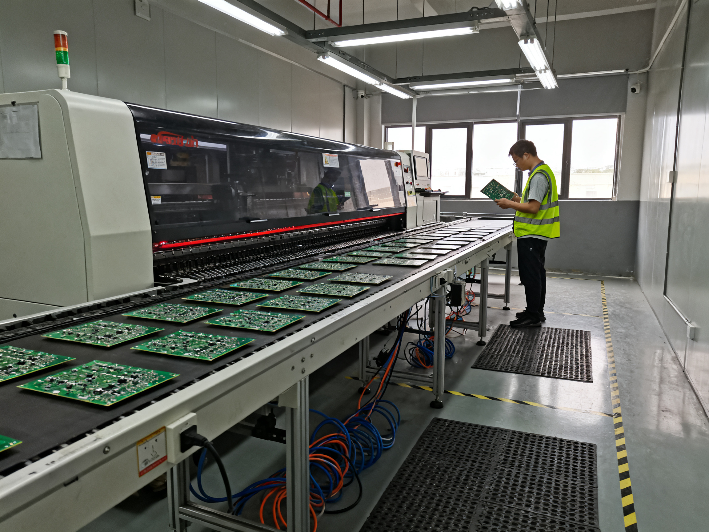
Written by Jace Liu. Jace has spent over 15 years in SMT manufacturing, working on production floors and in process engineering roles at major electronics assembly facilities across Asia and North America.## About the Author
Jace Liu is an SMT process engineering professional with deep roots in electronics manufacturing. With over 15 years of hands-on experience across production floors and process optimization roles at major assembly facilities, Jace brings practical insight into the daily challenges faced by SMT line operators and quality engineers.
His work has focused on lead-free reflow profiling, defect root cause analysis, and process window validation for high-volume manufacturing environments spanning consumer electronics, automotive, and industrial applications.
[Author bio placeholder: Add specific credentials, certifications (e.g., IPC-A-610 CIT/AIT), notable projects, or company affiliations before publication to strengthen E-E-A-T signals.]## What Reflow Soldering Defects Are Common?
Let me cut through the noise and give you a working definition. Reflow soldering defects are solder joint or assembly conditions created (or revealed) during the reflow process that fail to meet acceptance criteria, reliability requirements, or internal process control limits. They are not cosmetic blemishes you can wave away. Each one carries risk to function, durability, or safety.
Think about it this way. A cold joint might look ugly under magnification, but it can also cause intermittent electrical failures that are nearly impossible to trace. That is a defect. A tiny solder ball sitting near a trace might not cause an immediate short, but it can migrate over time and create reliability problems down the road. That is also a defect.
How Engineers Group These Defects
In practice, defects fall into six main categories based on what goes wrong:
| Defect Category | Common Examples | How You Spot It | Risk Level | Typical Fix |
|—————-|—————–|—————–|————|————-|
| Wetting defects | Dewetting, non-wetting, cold joints | Visual inspection, AOI | High | Adjust reflow profile, check pad cleanliness |
| Solder volume defects | Insufficient solder, bridging, beading | AOI, SPI | Medium to High | Revise stencil apertures, check paste deposit |
| Alignment defects | Tombstoning, component shift, rotation | AOI | Medium | Balance pad design, improve placement accuracy |
| Contamination defects | Solder balls, embedded foreign matter | AOI, X-ray | Low to Medium | Improve paste storage, reduce humidity |
| Thermal profile defects | Voids, head-in-pillow, graping | X-ray, cross-section | High | Optimize soak time, adjust peak temperature |
| Hidden joint defects | BGA opens, QFN thermal pad voids | X-ray, electrical test | Very High | Process recipe changes, nitrogen atmosphere |
The visible stuff you catch with AOI after reflow. Tombstoning, surface bridges, missing components, polarity mistakes. These are the defects that show up clearly under cameras and lights.
But here is what trips up a lot of teams. BGA and QFN packages hide their problems underneath the component body. You cannot see voids, head-in-pillow joints, or internal bridges with a camera. You need X-ray inspection, cross-sectioning, or electrical testing to find these issues.
Expert Tip: Not every imperfect-looking solder joint is a defect. IPC-A-610 acceptance criteria distinguish between conditions that are cosmetic versus those that actually threaten reliability. A slightly irregular fillet on a Class 1 consumer product might pass, but the same condition on an automotive control module would fail. Know your class, and prioritize accordingly.
The Hidden Defect Problem
I have seen production lines with excellent first-pass yields on AOI, only to discover significant hidden defect rates when they finally ran X-ray on their BGA assemblies. The camera said everything looked great. The X-ray told a different story.
That is why modern SMT lines use the inspection chain of SPI, AOI, X-ray, and ICT. Each tool catches what the previous one misses. Skip the X-ray step on your BGA boards, and you are essentially flying blind on your most critical joints.

For high-volume manufacturers in 2026, understanding which defects are visible versus hidden is not optional. It is fundamental to building quality into your process rather than trying to inspect it out later.## How to Identify Common Reflow Soldering Defects
Now that we know how engineers group defects, let’s get into the specifics. Each defect type has its own signature, its own risk profile, and its own way of hiding or showing up on your production line.
Bridging: When Solder Makes Unwanted Connections
Solder bridging happens when molten solder flows between adjacent pads and creates an unintended electrical connection. Under magnification, you will see a thin bridge of shiny metal connecting two separate circuit paths.
The problem here is obvious. A bridge is a short circuit. Your board might test fine at room temperature, but add some thermal cycling or vibration, and that bridge becomes a failure waiting to happen.
Fine-pitch components, like 0.4mm QFP packages, are particularly vulnerable. The pad spacing is tight, and if your stencil apertures are even slightly oversized, bridging becomes almost inevitable.
AOI systems catch most surface bridges after reflow. But if you have a BGA with internal bridging, you need X-ray inspection to find it.
Tombstoning: The Component That Stands Up on One End
Tombstoning, sometimes called the Manhattan Effect, is exactly what it sounds like. A passive component, usually a resistor or capacitor, lifts off one pad while the other end stays soldered. The component ends up standing upright, like a tiny tombstone.
This defect usually stems from imbalanced wetting forces. If one pad heats up and solders faster than the other, the surface tension difference pulls the component toward the cooler side.
I worked with a team once that kept getting tombstoning on 0402 capacitors. They blamed the solder paste for weeks. Turned out their QFN pads on one side of the component had slightly different thermal mass. The fix was as simple as adjusting the soak zone on their reflow oven.
Tombstoning is almost never cosmetic. A tombstoned component has significantly reduced mechanical strength and will almost certainly fail in the field.
Insufficient Solder and Cold Joints
Insufficient solder shows up as a fillet that looks thin, incomplete, or partially missing. The joint does not have enough molten metal to form a proper connection.
Cold joints look different. They have that dull, grainy appearance instead of the shiny, smooth surface you want to see. Cold joints happen when the solder did not melt completely or did not wet the pad properly.
Both of these defects compromise electrical conductivity and mechanical strength. Under IPC-A-610 criteria, cold joints are almost always unacceptable, especially for Class 2 and Class 3 assemblies.
Solder Balls and Solder Beading
Solder balls are tiny spheres of solder that scatter near the joint during reflow. They can migrate over time, and if they end up between two traces, you have a reliability problem.
Solder beading is similar but involves larger droplets that stick together. Both defects usually point to paste handling issues, high humidity in the production environment, or stencil design problems.
For consumer electronics with less stringent requirements, isolated solder balls that are far from active circuitry might pass as cosmetic. But for automotive or aerospace, even remote solder balls are usually not acceptable.
Voiding and Head-in-Pillow
Here is where we get into the hidden defect territory.
Voids are air pockets trapped inside the solder joint. On an X-ray image, they appear as dark spots inside the bright solder ball. Under IPC standards, voids exceeding 25% of the joint area are generally not acceptable for Class 2 and Class 3 products.
Head-in-pillow, or HiP, is a particularly sneaky defect. The solder ball on the component and the solder paste on the pad both melt, but they never fully merge. You get what looks like a connection from the outside, but internally there is a gap or weak interface.
HiP is nearly impossible to detect with AOI. You need X-ray, and sometimes you need cross-section analysis to confirm it.
For BGA packages, we have seen HiP defects escape visual inspection completely. The components looked perfect under the camera. The X-ray told a completely different story.
Dewetting and Non-Wetting
Dewetting looks like the solder started to flow but then pulled back, leaving irregular patches of solder with exposed pad visible underneath. Non-wetting is more extreme. The solder never adhered to the pad at all.
Both conditions usually indicate pad contamination, oxidation, or insufficient thermal input during reflow. These are process issues, not cosmetic ones.
Opens and Component Shift
An open is exactly what it sounds like. No electrical connection exists where one should. The solder never made contact with the pad.
Component shift means the part moved during reflow and ended up in the wrong position. If it is slightly off, you might catch it with AOI. If it is way off, you might have tombstoning or a missing component entirely.
Expert Tip: Not every imperfect-looking solder joint is a defect. IPC-A-610 acceptance criteria distinguish between conditions that are cosmetic versus those that actually threaten reliability. A slightly irregular fillet on a Class 1 consumer product might pass, but the same condition on an automotive control module would fail. Know your class, and prioritize accordingly.
Package-Specific Inspection Requirements
Different packages require different inspection approaches.
BGA and CSP packages hide their defects underneath the component body. You cannot see voids, HiP, or internal bridges with a camera. X-ray inspection is mandatory for these packages.
QFN packages have thermal pads on the bottom that are also hidden from view. Voiding under the thermal pad affects heat dissipation and grounding. If your QFN has wettable flanks, AOI can check the side fillets, but you still need X-ray for the bottom termination.
Fine-pitch assemblies need magnification and properly tuned AOI. If your AOI thresholds are too loose, you will miss bridging between closely spaced pads. If they are too tight, you will get false rejects that waste inspection time.
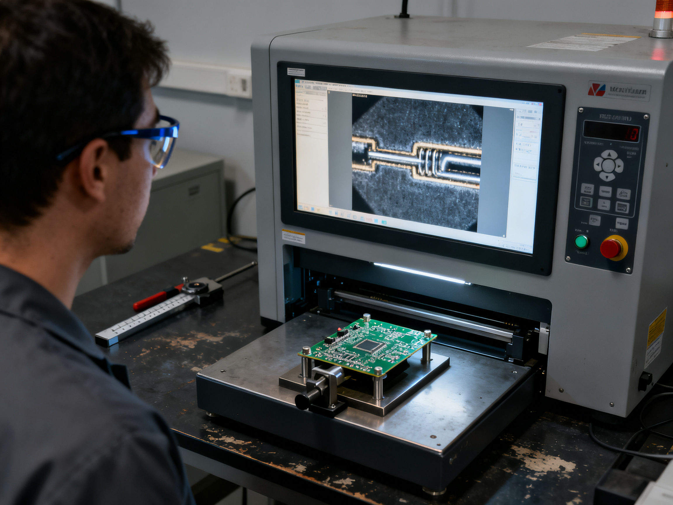
For high-volume lines in 2026, building the right inspection chain matters more than ever. SPI catches paste problems before reflow. AOI catches visible defects after reflow. X-ray catches the hidden defects that AOI cannot see. Skipping any step means defects will slip through.
Understanding what each defect looks like and where it hides is the foundation. But knowing what to do about it is where most teams struggle. That is what we will cover next.
What Causes Reflow Soldering Defects in High-Volume SMT Lines
So you have identified your defects. Now the real work begins. Figuring out why they happened in the first place. Here is the thing about reflow issues: the cause is almost never just one thing. It is usually a chain reaction. Something in your paste handling, your stencil design, your component placement, or your reflow profile did not quite line up, and the defect is the result.
Let me walk you through the full picture of what causes reflow soldering defects in high-volume SMT lines.
Root Causes Across the Full SMT Process
Defects can trace back to problems at almost every stage of your line. Here is how it breaks down:
Solder paste chemistry and storage
Paste that has been sitting too long, stored at the wrong temperature, or exposed to humidity loses its flux activity. The result? Poor wetting, cold joints, and non-wetting defects that look like oxidation problems but are actually paste degradation issues [1].
Stencil aperture design
Your stencil is where a lot of defects get started. Apertures that are oversized for fine-pitch components cause bridging. Poor area ratios mean incomplete paste release. And if your thermal pad apertures on QFN packages are not properly segmented, you will see voiding problems that nobody can explain [5].
Print quality and placement accuracy
Excess paste squishing out from misaligned prints creates bridges. Uneven paste deposits create tombstoning. And placement pressure that is too high can squeeze paste outside the pad boundaries, setting up reflow defects before the board even hits the oven [1].
Component solderability and PCB finish
Oxidized component leads, contaminated pads, or inconsistent ENIG finish thickness all create wetting problems. If your components have been sitting in stock too long, the solderability drops, and you get non-wetting even with a perfect reflow profile [2].
Oven profile, atmosphere, and conveyor stability
This is where most teams jump first when troubleshooting. The problem? The oven profile is often not the root cause. A profile that worked fine for six months and suddenly started causing defects usually means something upstream changed, not that your oven drifted [1].
Pro Insight: Before you touch your reflow oven recipe, check for process drift in the upstream stages first. Look at paste lot numbers and storage logs, review recent stencil changes, and verify paste deposit consistency with your SPI data. Nine times out of ten, the defect root cause is upstream of the oven, and changing your profile will just mask the real problem until it gets worse.
Connecting Defect Patterns to Likely Causes
Here is a quick reference for matching what you see to where it came from:
| Defect | Most Likely Root Cause | What to Check First |
|——–|———————-|——————–|
| Tombstoning | Thermal imbalance between pads, uneven paste volume | Reflow profile soak zone, pad copper balance, paste deposit uniformity |
| Bridging | Excess paste, misregistration, aperture design | Stencil apertures, print alignment, placement pressure |
| Voids | Flux outgassing, trapped volatiles, pad design | Reflow profile TAL, paste lot age, thermal pad aperture style |
| Non-wetting | Oxidation, poor solderability, insufficient thermal input | Component lead condition, PCB surface finish, peak temperature |
| Head-in-pillow | Flux exhaustion, oxidized surfaces, excessive preheat | Soak time and temperature, nitrogen atmosphere, component/package condition |
I ran a debugging sequence last quarter where tombstoning kept showing up on 0402 capacitors. We spent two days adjusting the reflow profile with no luck. The actual cause turned out to be a new stencil vendor whose aperture corners were slightly different geometry. The paste release was inconsistent enough to create uneven deposits that looked fine under SPI but caused tombstoning under reflow.
Why Lead-Free Narrows the Process Window
If you are still running leaded solder, here is something to consider. Lead-free pastes, especially SAC305 and SAC405 alloys, have smaller process windows than tin-lead did. The peak temperature needs to hit 240 to 250 degrees Celsius, the time above liquidus has to stay between 30 and 90 seconds, and thermal gradients across the board have to be tighter [4].
That higher peak temperature means more stress on moisture-sensitive components. It means greater sensitivity to component mass differences, where large BGAs and small resistors see different thermal profiles even on the same board. And it means tighter requirements for thermal uniformity across your reflow oven, typically plus or minus 1 degree Celsius [3].
For high-volume lines in 2026, lead-free is not optional for most product categories. But going lead-free without updating your process controls is a fast track to higher defect rates.
So now you know what causes these defects. But knowing the causes is only half the battle. What do you actually do about it? That is where most teams need the most help, and that is what we will cover next.## Reflow Profile Troubleshooting: Temperature, Time, and Atmosphere
A solid reflow profile is your first line of defense against solder defects. Get it right, and you prevent most problems before they start. Get it wrong, and you will spend weeks chasing issues that keep coming back no matter how many times you adjust the oven recipe.
Let us break down what each profile zone does and how errors in each zone create specific defects.
The Five Critical Zones of a Lead-Free Reflow Profile
For SAC305 and SAC405 lead-free solders, your profile needs to hit a peak temperature of 240 to 250 degrees Celsius with time above liquidus between 30 and 90 seconds [2][4]. Each zone serves a distinct purpose.
Preheat Zone
This is where you ramp from room temperature up to about 150 degrees Celsius at a rate of 1 to 3 degrees per second. The goal is gentle moisture removal without thermal shock. Too fast, and flux boils violently, creating solder balls that scatter across the board. Too slow, and paste slumps before it should, increasing bridging risk.
Soak Zone
Hold the board between 150 and 180 degrees for 60 to 120 seconds. This equilibrates thermal gradients across the assembly. Skip this zone or cut it short, and you get uneven heating that shows up as tombstoning on small components and head-in-pillow defects on BGAs [2][4]. The soak is not wasted time. It is where consistency gets built.
Time Above Liquidus
This is the window where solder is fully melted and wetting happens. Too short means incomplete melting, cold joints, and non-wetting. Too long allows excessive intermetallic growth that weakens joints over time [2][4].
Peak Temperature Zone
The highest point in your profile. Too low means poor wetting and dewetting. Too high risks component damage and creates a brittle joint structure. For lead-free in 2026, you are targeting 240 to 250 degrees at the hottest joint, but never exceeding what your most sensitive component can handle.
Cooling Zone
A rate of 2 to 4 degrees per second prevents thermal stress and controls grain structure. Slow cooling produces coarse grains that crack under thermal cycling. Fast cooling can warp boards and create microcracks [2][4].

| Profile Symptom | Likely Defect | Corrective Action |
|—————-|—————|——————|
| Slow preheat ramp (under 1 C/s) | Solder beading, slump bridging | Increase preheat gradient; check for cold spots in oven |
| Rapid preheat ramp (over 3 C/s) | Solder balls, flux spatter | Reduce preheat rate; verify thermocouple placement |
| Insufficient soak time | Tombstoning, HiP defects | Extend soak plateau; verify thermal uniformity across board |
| Peak too low (under 235 C) | Dewetting, non-wetting, cold joints | Increase peak temp within component limits; check zone calibration |
| Peak too high (over 255 C) | Component damage, IMC overgrowth | Reduce peak; verify component max ratings before running |
| Slow cooling (under 2 C/s) | Coarse grain structure, cracking | Increase cooling rate; check cooling zone configuration |
| Fast cooling (over 5 C/s) | Board warpage, microcracks | Reduce cooling rate; check conveyor speed |
Profiling High-Density Assemblies with Mixed Thermal Mass
Here is where things get tricky. A board with a large BGA next to a small 0402 resistor sees two completely different thermal profiles during reflow. The BGA mass holds heat. The resistor heats up fast. That difference creates stress and defect risk.
Board-level temperature differences need to stay within plus or minus 1 degree Celsius across critical joints for lead-free assemblies [3]. On complex boards, that means placing thermocouples on the highest mass component, the lowest mass component, and the center of the board. Some engineers also tag the corners, since those tend to run hot or cold depending on oven airflow.
Large shields, connectors, and press-fit components create similar headaches. They act as heat sinks, pulling energy away from nearby joints. For these, you either need a custom profile with slower ramp rates, or you need to add local preheating to compensate [2].
Pro Insight: Before you touch your reflow oven recipe, check for process drift in the upstream stages first. Look at paste lot numbers and storage logs, review recent stencil changes, and verify paste deposit consistency with your SPI data. Nine times out of ten, the defect root cause is upstream of the oven, and changing your profile will just mask the real problem until it gets worse.
The Atmosphere Question: Nitrogen or Air?
Modern reflow ovens give you the option of nitrogen atmosphere, and it genuinely helps for some applications. Nitrogen reduces oxidation on pads and leads, which improves wetting and reduces voids [1][5]. For fine-pitch assemblies and high-reliability products, it is worth the cost.
But here is the catch. Nitrogen also accelerates wetting speed, which can make tombstoning worse if your pad design or paste deposit is already imbalanced [5]. So before you blame the atmosphere, get your profile and paste deposit sorted first.
For high-volume lines running mixed products, look for ovens with 8 to 12 heating zones and plus or minus 1 degree thermal uniformity [1][3]. That gives you the flexibility to run delicate assemblies and robust products on the same line without constant recipe tweaking.
The key takeaway? Your profile is not a set-it-and-forget-it document. It needs validation with each new product, each material change, and each time defect patterns shift. Run profiling checks quarterly at minimum, and any time you see new defect trends showing up on your Pareto charts.## Which Reflow Defects Are Allowed Under Reflow Criteria?
Here is the question I get asked constantly on the production floor: “Is this a defect or not?” The honest answer? It depends.
Acceptability of reflow soldering defects is not a simple yes or no. It hinges on several factors working together. Your product class under IPC standards. What your customer specifically requires in their purchase order. The functional risk if that joint fails. Where the joint sits on the board. And how severe the condition actually is.
Defects, Process Indicators, and Acceptable Conditions
Not every imperfect solder joint is a defect. IPC-A-610 distinguishes between three categories that SMT engineers need to understand.
Acceptable conditions are joint appearances that meet all functional and reliability requirements. They pass without debate. A fillet that shows proper wetting and has adequate height, even if it is not perfectly symmetrical, often falls here.
Process indicators are conditions that do not meet ideal criteria but also do not threaten function or reliability. They might warrant process adjustment but do not require rejection. Minor surface texture variations that do not affect conductivity fall into this gray area.
Defects are conditions that fail acceptance criteria and require action. A joint with insufficient wetting that compromises mechanical strength, or a void exceeding 25% of the solder joint area on a BGA, these are defects under any interpretation.
| Condition Type | Voiding | Fillet Shape | Wetting Coverage | Surface Texture | Action Required |
|—————|———|————–|——————|—————-|—————-|
| Acceptable | Under 10% | Adequate fillet, slight irregularity | 75%+ coverage, good adhesion | Smooth, shiny finish | None |
| Process Indicator | 10-25% | Marginally low fillet | 50-75% coverage | Minor roughness | Monitor and adjust |
| Defect | Over 25% | Insufficient fillet height | Under 50% coverage | Cold joint appearance | Reject and rework |
| Customer Review | Any % in critical path | Any fillet issue on Class 3 | Any wetting shortfall on safety circuit | Any cosmetic issue on Class 3 | Escalate to engineering |
The 25% void threshold I mentioned comes from IPC-7095 standards for Class 2 and Class 3 assemblies. For Class 1 consumer products, isolated voids in non-critical locations might pass as acceptable if they do not affect function.
Expert Tip: Not every imperfect-looking solder joint is a defect. IPC-A-610 acceptance criteria distinguish between conditions that are cosmetic versus those that actually threaten reliability. A slightly irregular fillet on a Class 1 consumer product might pass, but the same condition on an automotive control module would fail. Know your class, and prioritize accordingly.
Class-Specific Requirements You Need to Know
Military, aerospace, automotive, and medical electronics operate under stricter rules than general consumer products. If you are building automotive control modules under IATF 16949, your defect thresholds are essentially zero. For aerospace assemblies, the bar is just as high.
What passes on a Class 1 consumer gadget might be completely unacceptable for a Class 3 medical device. The product class determines everything about how you classify and respond to each condition.
Bottom line: before you call something a defect or move it to the acceptable pile, know your class, check your customer specs, and assess the actual risk to function and reliability.## How to Prevent Reflow Defects: A Practical Process-Control Framework
The best way to handle reflow defects is to stop them before they happen. Catching problems after the oven means rework, scrap, and lost time. Prevention is a system. You need to control the entire process from paste selection all the way through to final inspection.
Here is a step-by-step prevention checklist that high-volume SMT lines use in 2026:
Prevention Checklist by Defect Type
Solder Bridging
- Optimize stencil apertures with 10-20% reduction from pad size for fine-pitch components
- Check print pressure and speed for consistent deposit
- Verify placement accuracy within 0.05mm tolerance
- Use rounded aperture corners to reduce paste drag
Tombstoning
- Balance copper distribution on component pads
- Ensure uniform paste deposit on both terminations
- Validate thermal profile for even heating across the component
- Check pad design matches component footprint
Voids
- Use low-voiding solder paste formulations
- Adjust profile to allow proper outgassing time above liquidus
- Segment thermal pad apertures on QFN packages
- Consider vacuum-assisted reflow for critical joints
Solder Beading
- Store paste in sealed containers at 2-10 degrees Celsius
- Maintain production area humidity below 45 percent RH
- Use paste within shelf life and follow FIFO rotation
- Never mix fresh paste with partially used material
Dewetting and Non-Wetting
- Verify pad cleanliness before printing
- Use nitrogen atmosphere for oxidation-sensitive assemblies
- Confirm reflow profile peak temperature meets paste specifications
- Check component lead solderability on incoming inspection
Head-in-Pillow
- Reduce preheat and soak time to preserve flux activity
- Use higher-activity paste for difficult surface finishes
- Minimize time between printing and reflow
- Control humidity in the production environment
BGA and QFN Hidden Defects
- Require X-ray inspection on all BGA assemblies
- Use segmented window-pane apertures for QFN thermal pads
- Specify Type 4 or finer powder for fine-pitch BGA packages
- Validate paste deposit volume with SPI before component placement
How Automated Lines Reduce Variation
Modern high-volume SMT lines use closed-loop inspection to prevent defects rather than just catch them after the fact. Here is the inspection chain that works:
- SPI catches paste problems before components are placed. If your stencil is worn or apertures are clogged, SPI tells you immediately instead of after reflow [3].
- AOI catches visible defects after reflow. Tombstoning, bridges, and missing parts show up clearly under cameras [3].
- X-ray sampling catches the hidden defects in BGAs and QFNs that AOI cannot see. For high-reliability products, you sample every board [1].
- MES traceability ties defect data to specific lot numbers, stencil batches, and line operators. When a problem shows up, you can trace it back fast [1].
- Oven monitoring continuously validates profile parameters against golden board data. Any drift triggers an alert before defects accumulate.
- Preventive maintenance keeps equipment performing consistently. Stencil wear, nozzle condition, and conveyor belt tension all affect defect rates if you let them drift.
From Our Experience: Last year we qualified a new automotive customer line. Tombstoning kept showing up on 0402 capacitors. We almost adjusted the reflow profile first. But instead, we checked the upstream stages and found the new stencil vendor had slightly different aperture corner geometry. The paste release was inconsistent enough to cause tombstoning under reflow. Fixing the stencil design solved the problem completely without touching the oven profile. The lesson here is simple: always look upstream before you touch the reflow recipe.
Integrated SMT lines with closed-loop process control see 60-80 percent reductions in rework and scrap [1]. That is not a small improvement. That is the difference between a profitable line and one that burns through margin on rework.
Building Your Prevention Framework
The framework covers eight control points:
- Design for manufacturability (DFM) review before production
- Material control with incoming inspection and storage protocols
- Solder paste handling and shelf-life management
- Stencil design and maintenance tracking
- Printer setup and SPI verification
- Placement accuracy and feeder maintenance
- Validated reflow profile with regular profiling checks
- Closed-loop inspection with escalation protocols
Each of these eight points feeds into the next. Miss one, and defects will find the gap. Get all eight working together, and you build a process that prevents problems instead of chasing them.## Troubleshooting Guide by Defect Type
Here is the section your production team has been waiting for. A no-nonsense lookup guide that tells you exactly what to do when you see a specific defect on your line.
Bookmark this page. Print it out. Put it next to your AOI station.
Quick-Reference Troubleshooting Table
| Defect | Probable Causes | First Checks | Prevention | Inspection |
|——–|—————–|————–|————|————|
| Solder Bridging | Excess paste, misaligned prints, oversized apertures | SPI paste volume data, stencil aperture dimensions, print alignment | Reduce aperture by 10-20%, check print pressure | AOI, X-ray for BGA bridges |
| Tombstoning | Thermal pad imbalance, uneven paste deposit | Reflow profile soak zone, pad copper balance, paste deposit on both terminations | Balance copper distribution, uniform paste volume | AOI |
| Voids | Flux outgassing, short TAL, paste age | Reflow TAL, paste lot age and storage logs, thermal pad design | Low-voiding paste, adequate TAL, segmented QFN apertures | X-ray |
| Solder Beading | Humidity contamination, poor paste storage | Production area humidity, paste storage temp, FIFO rotation | Store at 2-10C, humidity below 45% RH | AOI, visual |
| Dewetting/Non-wetting | Oxidation, insufficient heat, contamination | Pad cleanliness, peak temperature, component lead condition | Nitrogen atmosphere, verify peak temp, clean pads | AOI, cross-section |
| Head-in-Pillow | Flux exhaustion, oxidized surfaces, excessive preheat | Soak time, nitrogen use, time between print and reflow | Reduce preheat, higher-activity paste, minimize open time | X-ray, cross-section |
| BGA Opens | Non-wetting, pad contamination, excessive TAL | Component solderability, pad finish, profile peak | Verify component condition, adjust profile | X-ray, ICT |
| QFN Pad Voids | Thermal pad design, paste formulation, profile | Thermal pad aperture style, paste type, TAL | Window-pane aperture segmentation, low-void paste | X-ray |
Step-by-Step Troubleshooting Protocol
When you spot a defect on your Pareto chart, follow this sequence:
Step 1: Identify and quantify
Pinpoint the defect type, affected components, and approximate rate. Is it one board out of a thousand, or fifty out of a hundred? Numbers matter here.
Step 2: Check the easy stuff first
Look at your SPI data. Review recent paste lot numbers and storage logs. Did someone change stencil vendors recently? These upstream issues cause most defects that teams blame on the oven.
Step 3: Validate one change at a time
Here is where a lot of teams get into trouble. They change the reflow profile, swap the paste, and replace the stencil all at once. Then when the defect rate changes, they have no idea what fixed it. Pick one variable. Test it. Measure the result. Then move to the next.
Step 4: Document everything
Write down what you changed, when you changed it, and what happened. Include paste lot numbers, stencil batch IDs, and profile parameters. This documentation saves you hours of re-troubleshooting later.
Step 5: Know when to escalate
If the defect rate jumps suddenly without any material or process changes, call engineering. Do not keep running and hoping it resolves itself.
From Our Experience: We qualified a new automotive customer line last year. Tombstoning kept showing up on 0402 capacitors. We almost adjusted the reflow profile first. Instead, we checked the upstream stages and found the new stencil vendor had slightly different aperture corner geometry. The paste release was inconsistent enough to cause tombstoning under reflow. Fixing the stencil design solved the problem completely without touching the oven profile. The lesson here is simple: always look upstream before you touch the reflow recipe.
When to Escalate to Engineering
Some situations need more than line-side troubleshooting:
- Defect rates change dramatically with no obvious cause
- New component packages or pad designs are causing recurring issues
- Customer specifications conflict with your current process parameters
- You are considering profile changes that approach component temperature limits
Modern reflow ovens with closed-loop monitoring, like those from S&M Co. Ltd., can catch profile drift before it creates defects. If your oven lacks real-time monitoring, run profile verification checks every two weeks minimum.
The goal is not to become an expert on every defect. It is to have a system that helps you find the root cause fast, fix it properly, and document it so the next shift can handle the same issue without starting from scratch.
Equipment and Line Considerations for Reliable Lead-Free Reflow
Your reflow oven does not work in isolation. In 2026, modern SMT production requires thinking about your entire line as one connected system. Each piece of equipment affects the next, and decisions made at the oven station ripple through every other stage of assembly.
For high-density assemblies running lead-free solder, equipment specifications matter more than ever. Your oven needs enough zones to control thermal transitions smoothly. It needs tight uniformity so that a large BGA and a tiny 0402 resistor see consistent temperatures even on the same board. And it needs process monitoring that catches drift before it creates defects rather than flagging problems after boards have already gone through.
Here is a quick comparison to show what the difference looks like in practice:
| Capability | Basic Reflow Oven | Advanced Lead-Free Oven for High-Density Assemblies |
|————|——————|—————————————————–|
| Heating zones | 4 to 6 zones | 8 to 12 zones |
| Thermal uniformity | Plus or minus 2 to 3 degrees Celsius | Plus or minus 1 degree Celsius |
| Nitrogen atmosphere | Not available or optional | Standard or configurable |
| Cooling rate | 1 to 2 degrees per second | 3 to 5 degrees per second |
| Process monitoring | Manual profiling required | Real-time monitoring with alerts |
| Line speed capacity | Up to 0.8 meters per minute | Up to 1.4 meters per minute |
| Traceability | Basic logging | Full MES integration |
For automotive and aerospace manufacturers, traceability is not optional. IATF 16949 and defense electronics standards require you to tie defect data to specific lot numbers, line operators, and profile parameters. If a problem surfaces in the field, you need to trace it back to the exact board, the exact shift, and the exact oven recipe used. Basic ovens with manual logging cannot give you that level of detail quickly.
For BGA and QFN reliability, your oven needs to run profiles that support proper ball collapse without creating voids or head-in-pillow defects. That means adequate time above liquidus, controlled cooling rates, and consistency across the board. An oven with poor zone control will create subtle temperature differences that manifest as hidden defects you only discover during X-ray inspection or, worse, in the field.
From Our Experience: We qualified a new automotive customer line last year. Tombstoning kept showing up on 0402 capacitors. We almost adjusted the reflow profile first. Instead, we checked the upstream stages and found the new stencil vendor had slightly different aperture corner geometry. The paste release was inconsistent enough to cause tombstoning under reflow. Fixing the stencil design solved the problem completely without touching the oven profile. The lesson here is simple: always look upstream before you touch the reflow recipe.
When evaluating equipment for your SMT line, consider this checklist:
Equipment Selection Checklist for Lead-Free Reflow
- Does the oven have enough zones to handle mixed thermal mass assemblies?
- Is thermal uniformity within plus or minus 1 degree Celsius across the conveyor?
- Does the cooling system support controlled rates of 3 to 5 degrees per second?
- Is nitrogen atmosphere available for oxidation-sensitive assemblies?
- Does the monitoring system provide real-time alerts for profile drift?
- Can the oven integrate with your MES for full traceability?
- What is the maximum line speed, and does it match your production volume targets?
- How does the oven perform with your specific paste formulations and component types?
For large-scale manufacturers running consumer electronics, automotive controls, or military assemblies, buying equipment that matches only your current volume is short-sighted. Your line needs headroom for higher density products, tighter process windows, and tighter traceability requirements. Equipment vendors like S&M Co. Ltd. offer reflow ovens designed for these integrated SMT environments where the oven talks to the printer, the mounter, and the inspection systems in a closed loop.
The oven is the heat source, but the line is the product. Make sure your equipment investment supports the whole system.## Expert Takeaways for Reducing Reflow Soldering Defects
Here is what I want you to take away from this guide.
Most reflow defects are preventable when you control the full SMT process, not just the oven profile. I keep seeing teams spend weeks tweaking their reflow profile when the real problem started upstream at the stencil or paste storage. The oven is where defects show up. But the causes? Those usually live somewhere else entirely.
So when you spot a problem on your line, use this priority order:
- Identify the defect type and quantify the rate
- Confirm the acceptance criteria for your product class (Class 1, 2, or 3)
- Trace the root cause back through your process steps
- Adjust one variable at a time and measure the result
- Monitor through your inspection chain and track Pareto data
Simple. But not always easy.
From Our Experience: In high-volume SMT environments, I recommend prioritizing these defects first: BGA and QFN hidden defects (voids, HiP, opens), tombstoning on passive components, and any defect tied to a safety-critical circuit. These are the ones that hurt you in the field, not just on the AOI screen.
Before you scale up for high-density production in 2026, do this audit. Check your paste printing consistency with SPI data. Validate your reflow profile against current SAC305/SAC405 specifications. Confirm your inspection chain covers visible and hidden defects. And verify your reflow oven has the zone count, thermal uniformity, and process monitoring to handle tighter lead-free process windows.
Integrated SMT lines with closed-loop control see 60-80 percent reductions in rework and scrap. That is the gap between a profitable line and one that burns through margin on rework costs.
If you want help auditing your line or discussing reflow oven capabilities for high-volume lead-free production, reach out. We work with manufacturers running consumer electronics, automotive, and aerospace assemblies to tighten their process control and reduce defect rates.
The goal is not perfection. It is building a process that catches problems fast, fixes them properly, and keeps running without surprises.