
Published: November 16, 2026
Last Updated: November 16, 2026
Reading Time: 16 minutes (for a roughly 3,300-word technical guide)
Topic: SMT soldering process, reflow soldering process, and PCB warpage prevention
How to Prevent PCB Warpage During Reflow: A Step-by-Step Process Guide
Warpage is not a reflow oven problem. In most lines, it is a stack-up problem, a support problem, and a moisture problem that the oven simply reveals. This guide walks through how pcb warpage during reflow happens, what actually causes it, and the controls that stop it, so your SMT reflow process holds flat boards from incoming inspection through final inspection and rework.
A note on sources and standards: the figures and limits referenced in this guide are described in general terms so you can match them to your own board, component, and paste specifications. Always pull the exact acceptance criteria from the current edition of the applicable IPC, JEDEC, and component manufacturer documents before you set a production limit.
How to read this guide: if you are new to reflow, start with sections 1 through 3 and get the basics of the reflow soldering process step by step. If you already run a line and you are chasing a chronic warpage defect, jump to sections 2, 4, and 7, since those cover root cause, in-process controls, and troubleshooting.
What you will need on hand: the board stack-up drawing, the solder paste datasheet, the moisture sensitivity ratings for your components, a thermocouple or profiler for the oven, a warpage gauge or height measurement setup, and a copy of your current reflow profile.
What Actually Causes PCB Warpage During Reflow?
PCB warpage is not created by a single oven setting. It is the cumulative result of internal stresses acting on the board as its materials expand, soften, and cool at different rates. Understanding those mechanisms is the first step toward preventing the defect.
1. Asymmetric Thermal Expansion
During reflow, the entire assembly must heat the solder paste sufficiently for it to melt. Copper, FR-4, solder mask, components, and solder alloys do not expand at the same rate. If heat reaches one side of the board faster than the other, the two sides develop different thermal stresses.
Uneven heating can occur because of:
- Incorrect conveyor speed or oven zone dwell time
- Poor airflow or obstructed oven exhaust
- Differences in board thickness and component density
- Large copper features that create localized hot spots
- Boards stacked too closely during thermal conditioning
The result is temporary warpage while the board is hot. As the solder solidifies and the assembly cools, some of that deformation can become permanent.
2. CTE Mismatch Between Materials
Every material has a coefficient of thermal expansion, or CTE. When bonded materials expand by different amounts, the interfaces between them develop stress. This is especially important in multilayer PCB constructions, where copper and fiberglass alternate throughout the stack-up.
A heavily copper-weighted board may expand differently from a board dominated by FR-4. Changes in resin content, resin type, or copper distribution can therefore alter the board’s dimensional behavior even when two boards use nominally similar laminate.
3. Uneven Component Pull and Internal Stress
Large components can create mechanical forces during heating and cooling. Their packages, solder joints, and attachment areas may contract at rates that differ from those of the PCB. Thermal pads, exposed pads, leadframes, and large ground planes can further concentrate stress around individual components.
This is why a board with several large BGAs may behave very differently from one populated mainly with small passives—even if the two boards have similar outlines and reflow profiles.
4. Inadequate Board Support
A board must be supported in a predictable way as it passes through the oven. Without adequate support, the board can bow under its own weight, the weight of components, and the forces applied by conveyor rails or transfer mechanisms. Thin, large, or heavy boards are particularly vulnerable.
Common support problems include:
- Conveyor rails set too high or too low
- Missing or misaligned support pins
- Boards transferring between fixtures with different support heights
- Uneven spacing between palletized carriers
- High-temperature carriers that contact only one area of the board
Support is not merely a handling concern. It directly influences the stress state during the critical heating and cooling portions of the reflow process.
5. Solder Joint and Via Behavior
During reflow, solder changes from a solid to a liquid and then returns to a solid. The volume and mechanical state of solder joints can influence how the assembly deforms. Voiding, insufficient solder, poor fillet formation, and excessive joint volume can contribute to localized stress or movement.
For a BGA, warpage is especially consequential because small changes in package coplanarity can stretch or compress the solder-joint area. Underfill and stiffening features may improve package-level flatness, but they do not eliminate the need to control the board and reflow process.
Separate Thermal Stress From Process Instability
Not all deformation observed after reflow has the same cause. Production teams should distinguish between:
- Warpage caused by the assembly: Uneven expansion, CTE mismatch, component pull, or inadequate support
- Warpage caused by handling: Mechanical loading, conveyor misalignment, panel sag, or fixture transfer errors
- Warpage caused by reflow: An unsuitable thermal profile, excessive ramp rate, inadequate soak, or uncontrolled cooling
A useful investigation begins with the board’s condition at several checkpoints. Measure or inspect the assembly before reflow, immediately after reflow, and again after cooling. Compare those results with boards that have passed through the same line without defects.
Figure 2: The relationship between board construction, reflow conditions, and mechanical support determines whether temporary thermal deformation becomes permanent warpage.
Start With Measurement, Not Assumption
Visual inspection can identify a warped board, but it rarely identifies the dominant cause. For effective corrective action, measure the defect and document the process conditions at the same time.
At minimum, record:
- Board dimensions, thickness, layer count, and copper distribution
- Surface-finish and solder-paste specifications
- Component placement, package sizes, and thermal-pad details
- Oven zone temperatures, conveyor speed, and board loading pattern
- Support-pin locations and conveyor height settings
- Warpage magnitude and location measured before and after reflow
The key control point is not simply “the board came out flat.” It is whether the board remains within tolerance through heating, soldering, cooling, unloading, and downstream handling. A process that produces an initially flat assembly but leaves it highly stressed may still create reliability problems later.
In the next section, we will examine how to build a reflow profile that reduces thermal gradients while preserving solder-joint quality and production throughput.
1. Understand What PCB Warpage Is and When It Becomes a Defect Risk
Before you can control warpage, you have to name it correctly. Teams lose weeks chasing the wrong defect because “warped” gets used for three different problems. Here is the working vocabulary.
| Term | What it means on the shop floor |
| — | — |
| Bow | The board curves up or down along its longest axis, like a shallow smile or frown |
| Twist | The board is twisted diagonally, so one corner sits higher than the opposite corner |
| Static warpage | The shape the board holds after it cools and stays on the bench |
| Dynamic warpage | The shape the board has while it is hot inside the oven, which is usually larger than the final shape |
| CTE | How much a material grows when it gets hot. Copper, FR-4, and solder alloys each grow at their own rate |
| Tg | The glass transition temperature, where the resin in the laminate softens and suddenly stops behaving like a rigid material |
| Coplanarity | How flat a package sits relative to the board, measured across its leads or balls |
| Shadowing | A solder defect where a small part hides a large part from heat, so the joint on the far side never reflows properly |
Why the distinction matters: dynamic warpage is a process signal, static warpage is the inspection result. A board that bows 0.25 mm in the oven and settles to 0.10 mm on the bench passed. A board that bows 0.10 mm and stays there may still be a risk, because a bowed BGA can lose coplanarity with its own solder balls.
When does warpage become a defect? That depends on board length, thickness, component pitch, package type, and where the assembly sits in the process. A 300 mm panel with 0.8 mm FR-4 tolerates far more than a 150 mm board holding four fine-pitch BGAs. Your customer’s drawing and the current IPC or JEDEC document set decide the number. Pull those limits before you set a spec, not after the first scrap lot.
One more thing worth flagging: resin softening near Tg, copper imbalance across the stack-up, moisture swelling in the laminate, and uneven heating all push in the same direction. None of them is the sole villain, which is why the controls in the next sections work best as a system.
From Our Experience: The warpage we see most often on a line that “fixed” its profile and still shipped warped boards turned out to be copper imbalance plus a support pin missing from one corner, not the temperature curve. Once both were corrected, the same profile ran clean for months.
2. Identify the Root Causes Before Changing the Reflow Profile
Here is the trap most lines fall into. A board comes out of the oven warped, so somebody lowers the peak temperature by 5 degrees, runs a fresh lot, and hopes for the best. Sometimes it works. More often you just moved the problem somewhere quieter.
Warpage is a stack of interacting causes, so treat it like a stack, not a single line item. Group your suspects into six buckets before you touch a single setpoint.
Design and material. Asymmetric copper distribution, a mixed laminate stack-up, large cutouts and slots, thin board constructions, heavy copper on one side only, and uneven solder-mask coverage all set up the stress conditions that reflow then releases. Add heavy components such as large BGAs, QFNs with big thermal pads, and bottom-terminated connectors, and the board now has both a stress imbalance and a mass imbalance.
Storage and moisture. Laminate and component packaging absorb humidity from the air. When that moisture turns to vapor inside the oven, it pushes from the inside out. This is a strong candidate whenever warpage shows up on boards that sat in the shop for a few days before running.
Printing and placement. Solder paste volume, stencil aperture design, and heavy or uneven paste deposits change where mass sits on the board. A paste deposit three times heavier than its neighbors pulls the board out of plane during soak.
Oven and process. Conveyor speed, zone dwell, ramp rate, airflow balance, and repeatability across zones all shape the thermal gradient.
Tooling and support. This is where I would look first. Conveyor rails set too high, missing support pins, pallet spacing, and fixture transfer height differences all create mechanical load during the exact window when the board is softest.
Post-reflow handling. Cooling too fast, unracking boards too soon, stacking them warm, or dropping them into trays that press on the corners can create damage that looks like oven warpage but happened afterward.
Here is a simplified root cause map for PCB warpage during reflow:
                        PCB WARPAGE DURING REFLOW
                                   |
     +-------------+---------------+---------------+-------------+
     |             |               |               |             |
  DESIGN/       STORAGE/        PRINTING &      OVEN &       TOOLING &
  MATERIAL      MOISTURE        PLACEMENT       PROCESS      SUPPORT
     |             |               |               |             |
 Asym. copper   Floor-life      Paste volume   Ramp rate     Rail height
 Mixed stack   Over-bake       Stencil AP     Dwell time    Missing pins
 Cutouts        Humidity       Placement      Airflow       Pallet spacing
 Thin board     Component      weight         Zone repeat   Fixture transfer
 Heavy comps    packaging
 Solder-mask
Now match the symptom to the likely cause. Direction and location tell you a lot.
| Symptom | Probable causes | First thing to check |
| — | — | — |
| Upward bow (center high, edges low) | Asymmetric copper, heavy components on one side, uneven paste distribution | Copper balance in the stack-up drawing |
| Downward bow (center low, edges high) | Support raised at the edges, panel or rail contact points, thermal gradient across a wide board | Support pin heights and conveyor rail setting |
| Corner lift | Single-corner support gap, panel rail pressure, thermal gradient at one corner | Missing or misaligned support pin |
| Localized BGA or QFN deformation | Package-level warpage, thermal pad voiding, excessive paste on the pad | Package warpage spec and paste volume per pad |
| Panel edge distortion | Rail pressure, uneven pallet spacing, board not seated flat before entering the oven | Pallet and carrier setup on the line |
Expert Tip: Do not lower peak temperature as your first move. If the true cause is copper imbalance, a missing support pin, or moisture in the laminate, cooling the profile down will not fix it. It usually just gives you incomplete reflow, poor wetting, and voiding on top of the warpage you already had. Change one variable at a time, and change the variable that matches the symptom.
Before you move on, write down what you actually measured: board thickness and copper distribution, paste volume, support pin positions, and the symptom shape. That one page is what separates a real corrective action from a lucky profile change.
If your oven profile control is a bigger part of the problem than you think, it helps to look at how modern reflow ovens handle zone repeatability and profile storage, since that changes how much control you actually have over the thermal gradient.
3. Prepare the PCB, Components, Tooling, and Oven Before Reflow
Warpage control starts long before the board enters the oven. Most lines that fight warpage treat it as a thermal problem because the board comes out of the oven looking bent. But by the time you see it, the conditions that caused it are already locked into the material and the setup.
Three things have to be right before you fire the oven: the board, the moisture situation, and the mechanical support under the board.
Verify the incoming board
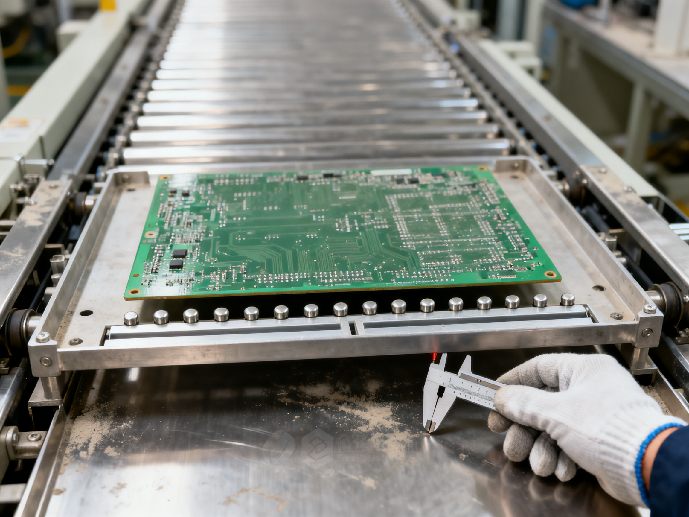
When a panel of boards arrives, check flatness before anything else. Set it on a granite surface plate and look for rock. If the bare laminate is already out of plane, no profile you write will bring it back. Also confirm thickness, layer count, and copper distribution against the stack-up drawing, and check laminate type and resin content so you know where the Tg sits.
Keep lot traceability. When warpage shows up on one lot and not another, and you cannot pull the lot history, you are guessing.
Control moisture
Humidity is the quiet cause behind a lot of sudden warpage problems. Laminate and component packaging both absorb water from the air. Store boards and reels in sealed, dry cabinets with a humidity indicator card, and respect the floor-life rules that come with your component packaging. When boards have been exposed longer than the limit, bake them per your supplier instructions and your paste vendor’s guidance, then let them cool in a dry environment before use.
Baking mistakes are expensive. Too hot and you can damage solderability or the resin. Too short and you have not removed the water. Get the bake time and temperature from the component supplier, and log it.
Choose the support method
Support is where most lines have the cheapest fix available. Match the method to the board.
| Support method | Ideal use case | Advantages | Thermal tradeoffs | Maintenance and cost |
| — | — | — | — | — |
| Center support pins | Thin boards, high-density panels | Low contact area, minimal heat loss | Pins can act as heat sinks on large copper areas | Low cost, pins need regular height checks |
| Edge rails | Standard rectangular boards, moderate thickness | Simple, fast changeover | Continuous rail contact cools edges unevenly | Low to medium cost, frequent adjustment |
| Carrier pallets | Panelized boards, double-sided assembly | Protects underside components, keeps boards flat | Pallet mass changes soak time and ramp | Medium cost, pallet inventory and refurbishment |
| Mesh belt | Small boards, selective or blanking lines | Light, flexible, good for mixed sizes | Low thermal mass, can let boards bow between nodes | Medium cost, belt tension needs monitoring |
| Dedicated fixtures | High-volume, high-warpage-risk products | Best repeatability, custom contour | Fixture must match the board outline | Higher cost, needs its own preventive maintenance plan |
From Our Experience: On a line we supported with a generic pallet, the pallet’s thermal mass was extending soak time enough to let the resin soften further before the solder melted, which added to the bow. Swapping to a lighter carrier and adding four center support pins fixed the defect without touching the profile at all.
Pre-reflow readiness checklist
Before you release the lot, confirm each line:
- Incoming board flatness checked and within the supplier’s limit
- Stack-up, thickness, and copper balance match the released drawing
- Storage and floor-life records available for boards and components
- Required bake completed and documented where needed
- Support pins present, clean, and at the correct height
- Conveyor rail height set and verified against the board underside
- Components checked for bottom-side clearance and heat-sensitive parts
- Oven zone readings and conveyor speed match the released profile
- Warpage measurement method and sampling plan defined for this lot
Check the oven too
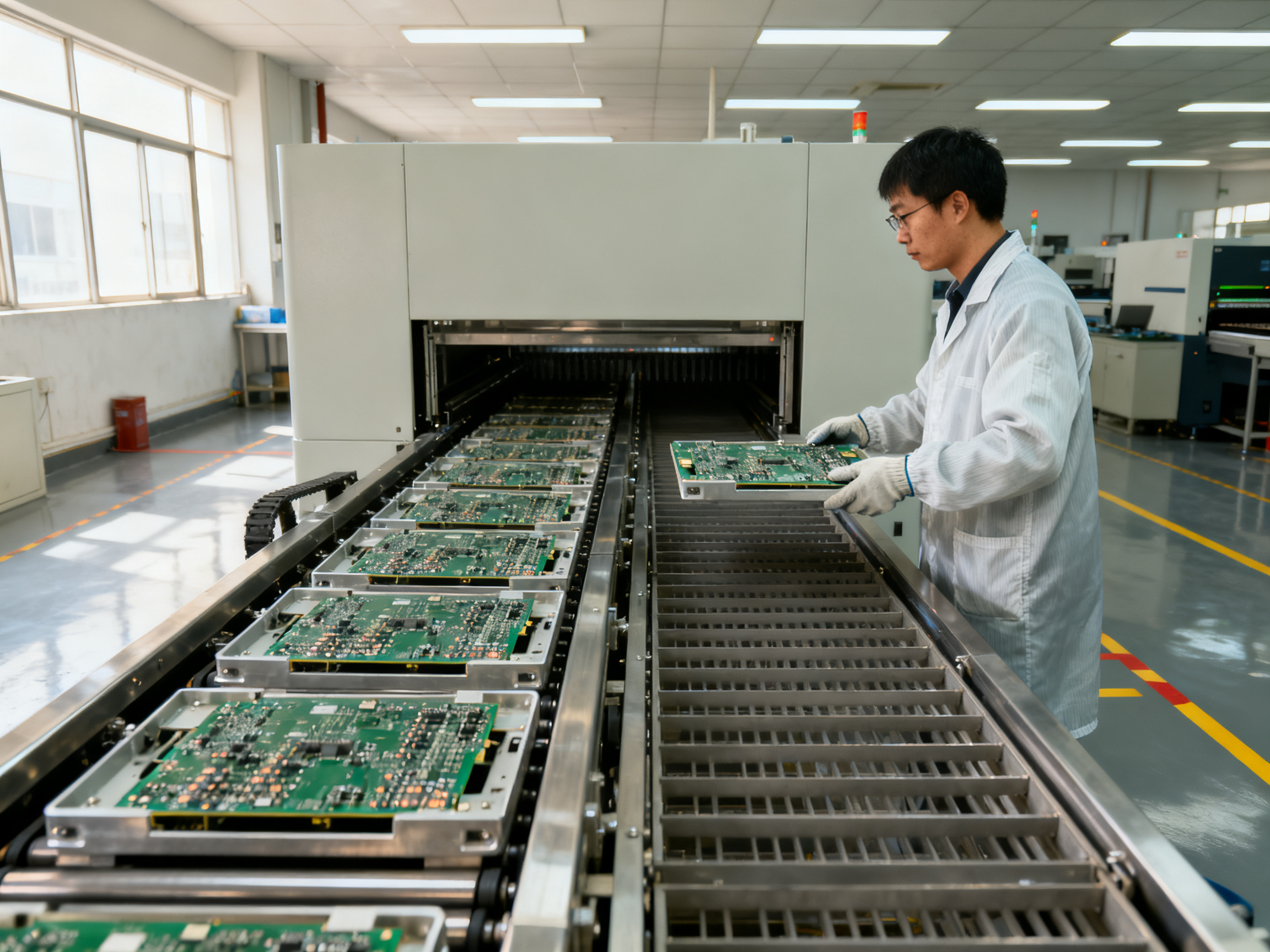
Run a quick empty oven check before the first board. Look at zone setpoints against actual readings, confirm airflow and exhaust are not blocked, and verify conveyor speed. A single blocked exhaust duct can flatten the thermal gradient across the whole width of the conveyor, and that is a real source of twist.
If your line runs multiple products, keep a stored profile for each assembly and confirm the oven recalls it correctly. Multi-zone reflow ovens with repeatable zone control and profile storage make this far easier to manage, and that matters once you are chasing a chronic warpage defect.
The point of all of this is simple. Reflow reveals the board’s condition; it rarely creates it. Prepare the material, the moisture, and the support, and the profile has a much easier job to do.
4. Reflow Sololdering Process Step by Step: Controls That Minimize Warpage
Now we get to the part everyone thinks is the whole answer. Walking the reflow soldering process step by step, in order, is where a stable profile turns into a flat board, provided the mechanical setup from section 3 is still holding.
Expert Tip: Every target in this section comes from three documents, not from memory or from a colleague’s oven recipe: the solder paste datasheet, the laminate data sheet, and the component manufacturer’s reflow classification. There is no single temperature recipe that is safe for every assembly. A SAC305 paste with a wide process window on a 1.6 mm FR-4 board with lead-free BGAs behaves nothing like the same paste on a thin flex laminate with a 260 °C-class part on it. Write the limits down before you profile.
The six-step reflow soldering process step by step
Step 1: Confirm the recipe and the loading. Load the released profile for that specific assembly, not the one sitting next to it in the oven memory. Check board orientation, conveyor rail width, support pin positions, conveyor speed, and the gap between assemblies on the pallet. Spacing matters more than people expect. Boards packed shoulder to shoulder create a thermal shadow, so the leading edge of one board runs hotter than the trailing edge of the next. That is a reliable source of twist across the panel.
Step 2: Preheat. Bring the assembly up toward soak gradually and uniformly. The goal is to remove the last of the moisture in the laminate and to bring the whole board to temperature without shocking the copper. Too fast here and the surface reacts before the core does.
Step 3: Soak. Hold the assembly in a temperature band above the solder paste’s flux activation point and below the liquidus of the solder alloy. This is where the board reaches a relatively uniform temperature and the resin softens near Tg. A long soak equalizes temperatures; a short one leaves a thermal gradient that becomes bow.
Step 4: Reflow. Bring the assembly to peak so the solder alloy reaches its liquidus and wets the lands. Aim to satisfy the paste datasheet’s time-above-liquidus window without adding unnecessary seconds at peak. Every extra second at peak is extra time with a softened laminate and a liquid board, and that is where warpage is made.
Step 5: Cooling. Bring the assembly down through the solder solidification range at a controlled rate, and control the top-to-bottom difference as well as the front-to-back one. Abrupt cooling on the underside while the top is still hot is a common twist generator. Fan settings, zone airflow, and cooling profile entries all matter here.
Step 6: Unload and handling. Keep the assembly supported until it is mechanically stable. Do not stack, unrack into a tight tray, or press on the corners while the board is still warm. A board that comes out of the oven flat and gets bent in the unload tray still counts as a warped board at final inspection.
REFLOW SOLDERING PROCESS: SIX STEPS
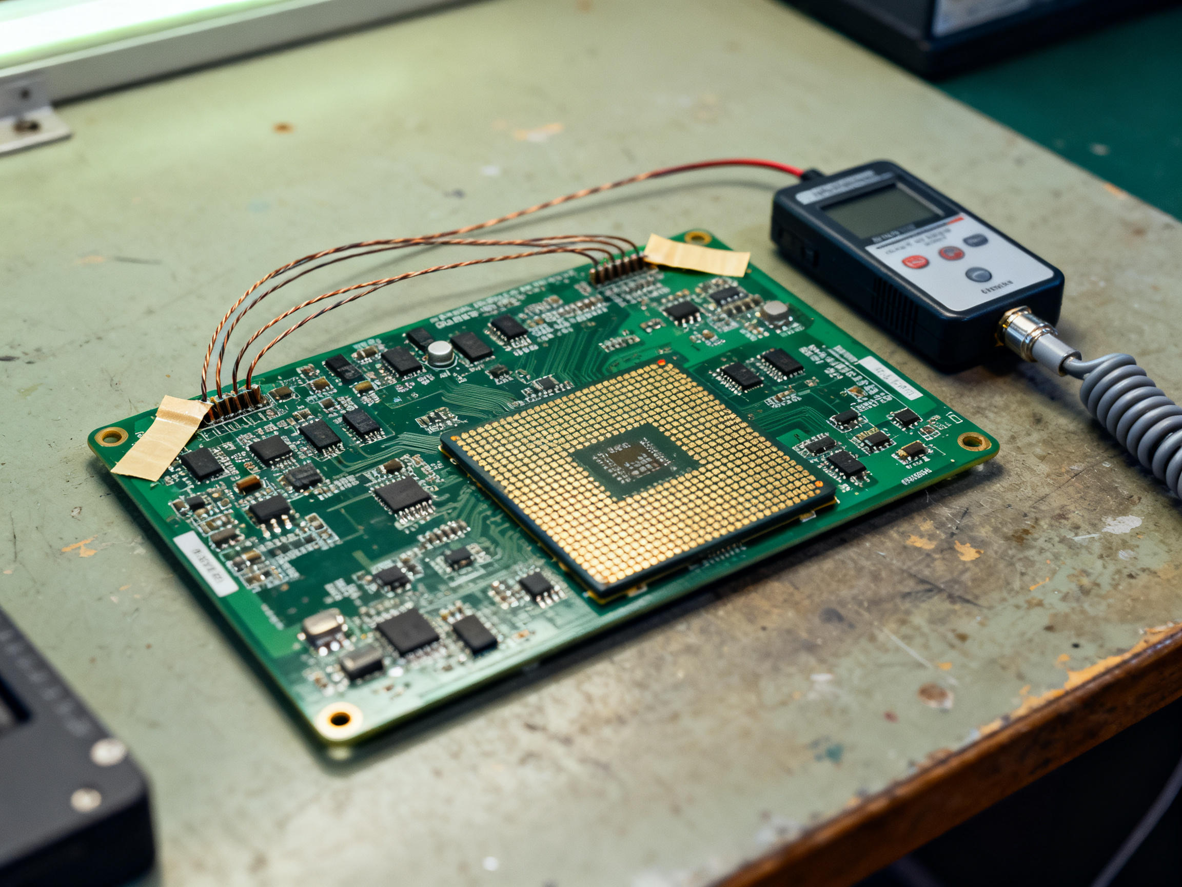
 1. Recipe + loading check   -> board orientation, rails, pins, spacing
 2. Preheat                  -> gradual, uniform ramp, moisture removal
 3. Soak                     -> equalized temperature, resin softens
 4. Reflow                   -> peak + time above liquidus, controlled
 5. Cooling                  -> controlled gradient, solder solidifies
 6. Unload + handling        -> supported until stable, no hot stacking

 WARPAGE RISK
   HIGH  |  #4  #5   <- peak dwell + cooling gradient
         |  #2  #3   <- ramp rate + soak balance
         |  #1  #6   <- loading pattern + hot handling
   LOW   |  balanced profile + verified loading + support
Parameters to verify before you run anything
| Parameter | Verify from | Risk if too low | Risk if too high |
| — | — | — | — |
| Ramp rate | Paste datasheet, board thickness and size | Flux may not activate, solder balls and incomplete wetting | Laminate delamination, copper stress, thermal shock |
| Soak temperature and time | Paste datasheet plus component floor-life data | Non-uniform board temperature, cold joints, poor activation | Resin softens too long, package and board stress build |
| Peak temperature | Solder alloy liquidus in the paste datasheet | Incomplete wetting, weak fillets, poor joint formation | Component damage, intermetallic growth, board weakening |
| Time above liquidus | Paste datasheet process window | Poor wetting, insufficient joint formation | Excess copper dissolution, long stress window at peak |
| Cooling rate | Component solderability rating, board mass | Uneven solidification, joint cracking risk | Warpage and twist from top-to-bottom gradient |
| Conveyor speed and spacing | Oven capacity, oven length, board footprint | Over-soak and board overheating | Under-soak, cold joints, reduced throughput |
Everything in this table has a matching specification somewhere in your supplier paperwork. If you cannot point to the source document for a number, that number is a guess.
Equipment helps more than people expect here. Multi-zone reflow ovens with independent top and bottom airflow control, per-product profile storage, and logged recipe data give you a much tighter grip on the thermal gradient that drives bow and twist. S&M Co. Ltd. builds lead-free reflow ovens and full SMT lines for high-density consumer electronics, semiconductor, and military work, and the repeatable zone control is what makes the six steps above verifiable rather than hopeful.
One last thought before the next section. A perfect profile cannot rescue an unbalanced stack-up, but a bad profile will ruin a well-built board every single time. Get the profile right for this assembly, with this paste, on this laminate. Then keep it there.
Section 5 preview: in the next section we build and validate the actual profile, using thermocouple placement, delta-T checks, and a design of experiments so the recipe is backed by data rather than habit.
5. Build and Validate a Reflow Profile for the Actual Assembly
A reflow profile belongs to one assembly, one paste, one laminate. The oven is just the tool that runs it. So build the profile against the board you actually ship, and validate it every time the recipe changes.
Place your thermocouples where the board actually warps
Most lines put two probes on a small board and call it done. That tells you the average temperature and nothing about the gradient that causes bow and twist.
Attach at least three, and spread them across the board so you capture the extremes:
THERMOCOUPLE PLACEMENT (TOP VIEW, TYPICAL)
 +--------------------------------+
 | TC1 corner        TC3 corner   |   TC1/TC2 = corners (twist)
 |   o                            |   TC3/TC4 = center line (bow)
 |                                |
 |         o TC2 center            |   TC5 = heavy copper / heat sink
 |                                |   TC6 = near large BGA or QFN
 |            o TC4 center         |
 |                                |
 | TC6 near BGA    o TC5 heavy Cu  |
 +--------------------------------+
 Secure with Kapton tape, not clips.
Two corners on a diagonal reveal twist. Two points on the centerline reveal bow. One probe on a large exposed-pad QFN tells you whether that package is running hotter than the rest of the board, which is usually the difference between a good joint and a void.
Measure delta-T, then check every location against the window
Delta-T is the spread between your hottest and coldest thermocouple during the ramp and soak region. A large delta-T means the board is not behaving as one piece, and that is where warpage starts.
Hold every location against three limits at once:
- The solder paste’s allowed ramp rate, soak range, and time above liquidus
- The component manufacturer’s peak temperature classification
- The laminate’s glass transition temperature and decomposition rating
If one probe fails a limit, the profile fails, even when the others look good. That is the whole point of placing six probes instead of two.
Record the validation, then run it like an experiment
Keep a signed record for each released profile. Then, if you still have warpage, change one variable at a time.
| Variable | Setting A | Setting B | Why test it |
| — | — | — | — |
| Conveyor speed | 80 cm/min | 100 cm/min | Sets total time above Tg in the oven |
| Zone 2 (soak) setpoint | 150 °C | 165 °C | Changes how long resin stays soft |
| Support method | Edge rails | Center pins | Changes mechanical load while hot |
| Board orientation | Component side up | Component side down | Changes which side sees heat first |
Document every run: recipe revision, board lot, support method, loading pattern, oven ID, and the defect result. Ten documented runs beat a hundred guesses, and the record is what you hand to the next engineer.
From Our Experience: On one board we profiled two thermocouples and called it done for years. When we finally added probes at the corners and next to the large BGA, the delta-T turned out to be 18 °C across the panel, mostly caused by boards running shoulder to shoulder on the pallet. Spacing them out removed the twist. No profile change was needed at all, which is exactly why we now profile first and adjust the profile last.
In 2026, most modern reflow ovens will store profiles per product and log the thermal data for each run, so keeping these records is a matter of exporting files rather than hunting for a notebook. S&M Co. Ltd. builds lead-free reflow ovens and full SMT lines with per-product recipe storage and repeatable zone control, which is what makes a validation record worth keeping in the first place.
Section 6 preview: next we look at cooling control, where a lot of the twist you are seeing actually gets created, after the solder has already melted.
6. Measure PCB Warpage During Reflow and Confirm Process Capability
A board can look flat on the bench and still be misbehaving. What matters is the shape it holds across the whole heat cycle, so your measurement plan needs to separate two different questions. Room-temperature flatness tells you whether the board passed inspection. Dynamic measurement tells you whether your process is actually controlling stress.
| Method | Typical accuracy | In-process use | Speed | Cost | Main limitation | Best use |
| — | — | — | — | — | — | — |
| Surface plate and height gauge | 0.02 to 0.05 mm | Bench or post-reflow | Slow, manual | Low | Static only, setup dependent | Final inspection and first-piece checks |
| Shadow moiré | 0.01 to 0.02 mm | Near-line or lab | Medium | Medium | Needs fixturing and a clear optical path | Fast twist and bow screening |
| Digital image correlation | 0.005 to 0.02 mm | Bench or in-oven with camera | Fast | Medium to high | Surface texture and calibration required | Full-field shape, strain coupling |
| Laser or optical profilometer | 0.005 to 0.01 mm | Offline | Fast | High | Line of sight, reflective surfaces | Package and pad coplanarity work |
| In-line inspection camera | 0.02 to 0.05 mm | Yes, directly in the line | Fast | High | Tied to line speed and lighting | Trend monitoring on high-volume lines |
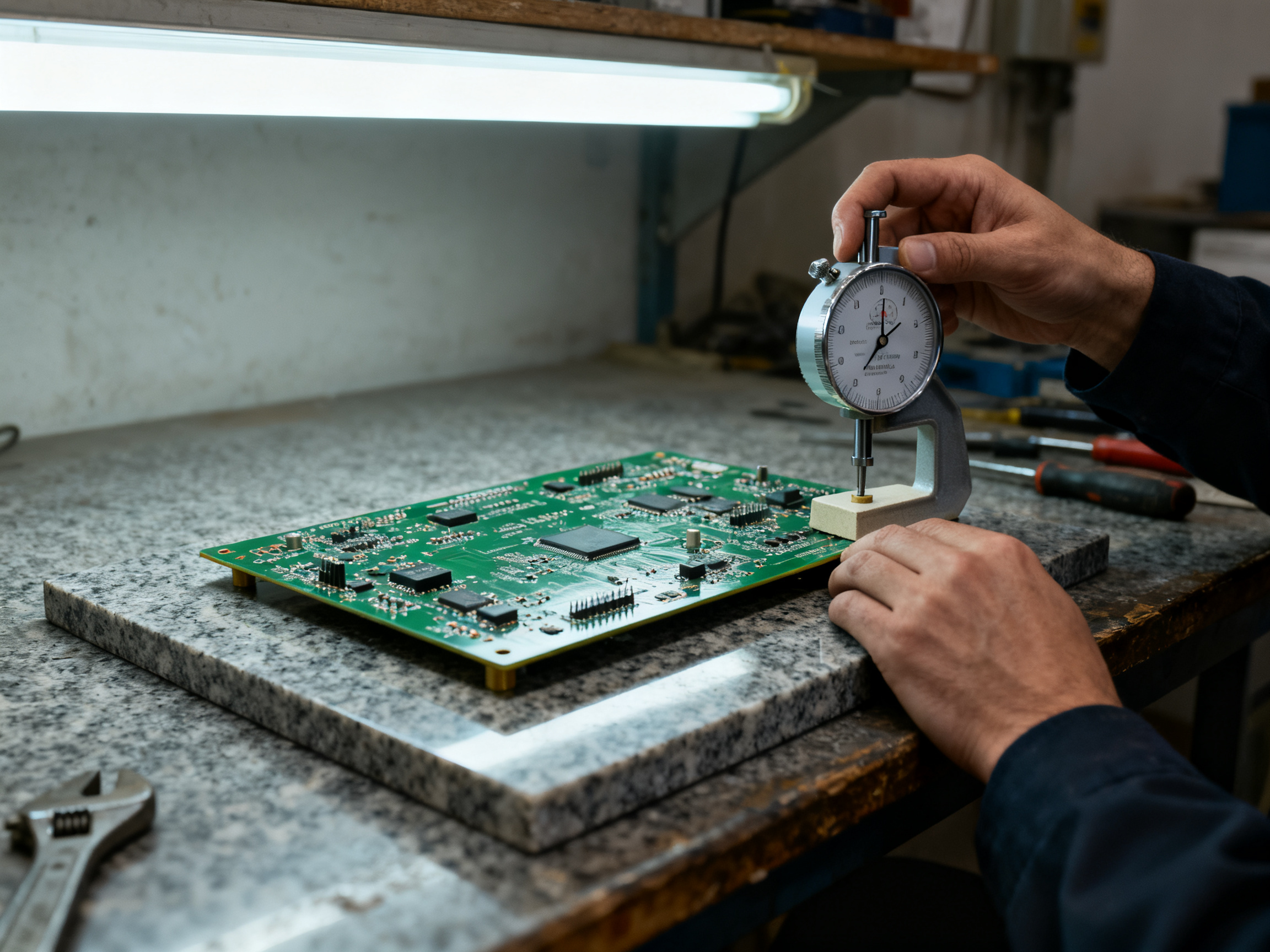
Pick the cheapest method that answers your actual question. For most lines, that means a calibrated height gauge on a granite surface plate for final inspection, plus shadow moiré or a camera check for boards you suspect are still moving while hot.
WARPAGE MEASUREMENT PLAN
  Final inspection   -> surface plate + height gauge (every lot, sampled)
  Suspect boards     -> shadow moire or DIC (full shape, dynamic if hot)
  Packages           -> optical profilometer (coplanarity at BGA/QFN)
  Trend view         -> in-line camera (Cpk per product, per shift)
Build the validation plan around four checkpoints. First-piece approval gates the start of a lot. Lot sampling catches drift before it reaches the customer. Critical package inspection links board flatness to BGA and QFN coplanarity, since a small bow can ruin a fine-pitch joint even when the board passes a generic flatness limit. AOI or X-ray correlation ties the warpage number to actual solder condition, so the limit you publish reflects defects rather than opinion.
Set a reaction plan in advance. If average warpage on a lot trends up, or if one package type starts failing, everyone knows who must respond and when the line should stop. That is what makes PCB warpage prevention a process control rather than a hope.
For the thermal side of the same story, watch reflow-oven temperature uniformity across the conveyor width in your profile records. A process can hold a perfect average and still create twist.
Section 7 preview: Next, we cover troubleshooting persistent warpage and how to decide when a rework attempt creates more risk than a controlled scrap or an engineering disposition.
8. A Three-Step Warpage Control Plan for the Next Quarter
Reducing recurring warpage requires a controlled improvement cycle rather than another one-time profile adjustment. Use the following three-step plan to move from diagnosis to verified control. Assign an owner and a target date to each step, review results at a fixed interval, and avoid introducing more than one uncontrolled change at a time.
Step 1: Establish a Reliable Baseline
Start by documenting the current process and proving that the measurement system can detect meaningful differences.
- Select a representative board family and define a repeatable warpage measurement method, including sample quantity, measurement locations, equipment, and acceptance criteria.
- Record initial data across multiple boards, lots, shifts, and oven positions. Separate mean warpage from variation so that a stable average does not hide an intermittent tail defect.
- Verify support conditions, component placement symmetry, reflow recipe, conveyor loading, and oven uniformity. Record every relevant factor so future trials have a clear reference point.
- Classify failures by type, such as bow, twist, corner lift, or warpage that appears only after cooling. This prevents different mechanisms from being treated as one problem.
The baseline is complete when someone else can repeat the measurement and obtain comparable results. If operators disagree about which boards fail or where the maximum warpage occurs, fix the measurement method before changing the process.
Step 2: Correct the Dominant Cause
Use the troubleshooting sequence from section 7 to identify the most likely mechanism, then test one corrective action at a time.
- Correct measurement, loading, support, or material conditions that are outside control.
- Run a controlled trial using the smallest practical sample that still represents normal production variation.
- Compare trial results with the baseline using the same measurement method and acceptance criteria.
- Expand the trial gradually while checking for new defects, including solder-joint anomalies, insufficient reflow, component movement, or laminate damage.
- Document any adverse tradeoffs and obtain engineering approval before adopting a permanent process change.
Prefer reversible corrections before changing the thermal profile. Adjust orientation, spacing, support methods, conveyor speed, airflow, cooling, or bake exposure before modifying the recipe. If a profile change is necessary, validate it through the profiling method from section 5 and establish clear operating limits for the entire acceptable process window rather than relying on one nominal setting.
Pro Insight: A successful trial is not proof of a robust process. A correction that works on one pallet, lot, or shift may still be sensitive to loading, humidity, oven aging, or maintenance drift. Challenge the result under representative conditions before treating it as permanent control.
Step 3: Lock In the Result and Prevent Recurrence
Once the corrective action is proven, convert the result into a controlled process that is easy to follow and audit.
- Update the control plan with the verified recipe, loading pattern, support configuration, measurement frequency, and escalation criteria.
- Train operators on the fault signatures they are expected to identify and the actions they are permitted to take.
- Add a response plan for boards held beyond their exposure limit, racks loaded incorrectly, support pins missing, or oven zones drifting outside uniformity checks.
- Track key process indicators by lot, product, oven, shift, and maintenance event. Review trends rather than reacting only to individual failures.
- Schedule periodic confirmation runs using retained samples or controlled boards. Recheck after major maintenance, recipe transfers, material or component changes, and seasonal shifts in humidity.
Close the quarter with an engineering review. Compare the original baseline with the validated process, document residual risk, and assign actions for any remaining variation. Keep rejected or marginal approaches in the troubleshooting record so the organization does not repeat ineffective trials.
Quarterly Scorecard
A concise scorecard makes the improvement visible and keeps the effort focused:
| Measure | Purpose |
| — | — |
| Warpage pass rate | Shows whether the process consistently meets specification |
| Mean and maximum warpage | Separates overall improvement from severe outliers |
| Changeover and seasonal trend | Reveals sensitivity that short trials may miss |
| Rework and scrap rate | Confirms that warpage reduction does not create new quality costs |
| Time to containment | Measures how quickly abnormal boards are identified and isolated |
| Control-plan compliance | Confirms that operators are following the validated method |
Do not optimize for the lowest measured warpage alone. The goal is a capable, repeatable process that meets requirements without introducing soldering, handling, or reliability defects.
S&M Co. Ltd. provides lead-free reflow ovens and full SMT lines with logged per-product recipes, repeatable zone control, and traceable process data. These capabilities support baseline measurement, controlled trials, and ongoing verification, making improvements easier to sustain across shifts and production sites.
8. Standardize PCB Warpage Prevention Across High-Volume SMT Lines
A fix that works on one line rarely survives a second line, a second shift, or a second oven. That is the gap this section closes. Once you have a validated setup, the real work is converting it into something every operator, every shift, and every site can follow without asking you in person.
Standardization in PCB warpage prevention means turning a working trial into a controlled recipe, a fixture requirement, an inspection frequency, and a written reaction plan. If it only lives in one engineer’s head, it is not a process yet.
One-page implementation checklist
- Controlled recipe per product, with revision number and the source document behind every limit
- Setup photos for fixture, support pin positions, board orientation, and pallet spacing
- Fixture and support pin maintenance interval, plus a replacement spare set
- Acceptance criteria and sampling frequency for incoming and post-reflow warpage
- Operator reaction plan stating who to call, what to quarantine, and what to check first
- Revalidation triggers: material change, oven maintenance, seasonal humidity shift, or supplier swap
Who owns what
| Function | Role | Key warpage responsibility |
| — | — | — |
| Design engineering | A | Stack-up copper balance, panelization, heavy component placement |
| Procurement | I | Supplier clauses for board flatness, laminate spec, packaging |
| Supplier quality | R | Incoming flatness, moisture packaging, floor-life records |
| Incoming quality | R | Lot sampling and flatness verification on receipt |
| SMT process engineering | A | Profile, support method, loading pattern, control plan |
| Maintenance | R | Support pin height checks, oven uniformity, airflow and exhaust |
| Production | R | Setup execution, handling, unload and cooling discipline |
| Quality | C | Measurement system, disposition, defect correlation |
Leading indicators beat defect yield. Track board flatness at incoming, moisture exposure hours, delta-T, profile window index, oven alarms, and fixture condition. These move before the defect rate does.
Standardization also means deciding what happens when a setting changes. Any new laminate, paste, component, or fixture needs a short revalidation run, not a quiet substitution. Documented recipes and logged process data, as available on modern multi-zone reflow ovens, make that check quick rather than theoretical.
When you roll this out across lines, keep one simple rule: if the operator cannot run the setup from the page alone, the page is incomplete. Fix the page, then the setup.
Conclusion: Prevent Warpage by Controlling the Whole Thermal System
Warpage control is a sequence, not a single fix. Verify the materials, control moisture, support the board, profile the actual assembly, measure dynamic behavior, then standardize the validated recipe. The best outcome balances board flatness with solder-joint quality, throughput, component temperature limits, and long-term reliability.
Your next step: audit one high-defect product using this checklist and set a measurable baseline before touching the recipe.
- [ ] Incoming board flatness checked against the supplier limit
- [ ] Stack-up copper balance and thickness confirmed
- [ ] Moisture exposure hours and bake records available
- [ ] Support pins present, clean, and at the correct height
- [ ] Profile validated with three or more thermocouples and delta-T logged
- [ ] Warpage measurement method and sampling plan defined
- [ ] Control plan updated with recipe, support, and reaction criteria
Need a second set of eyes on your oven or line setup? S&M Co. Ltd. builds lead-free reflow ovens and complete SMT lines with per-product recipe storage, repeatable zone control, and traceable process data, and we support reflow profiling consultations and line-configuration reviews for high-volume SMT operations.