You can dramatically improve wave soldering results by focusing on five proven methods: optimizing process parameters, maintaining equipment, selecting the right solder and flux, refining PCB design, and strengthening inspection routines. In poorly optimized conditions, up to 50% of PCB defects can stem from wave soldering issues. When you apply best practices, you can see impressive gains, like increasing first pass yield from 85% to 96% and cutting cold joint defects by 25%.
By using these techniques, you gain higher quality, fewer defects, and more reliable assemblies.
Key Takeaways
-
Control temperature carefully during wave soldering to avoid cold joints and damage. Use proper preheat and solder pot temperatures and monitor with thermal tools.
-
Keep equipment clean by following daily, weekly, and monthly maintenance schedules. Regular cleaning reduces defects and improves solder joint quality.
-
Choose the right solder and flux materials that match your process and clean properly. Fresh, compatible materials help create strong, reliable joints.
-
Design PCBs with proper component alignment and pad spacing to ensure even solder flow and prevent defects like bridging or open circuits.
-
Perform thorough visual inspections and use automated tools to catch defects early. Strong quality control and operator training reduce rework and improve yields.
Process Parameters
Temperature Control
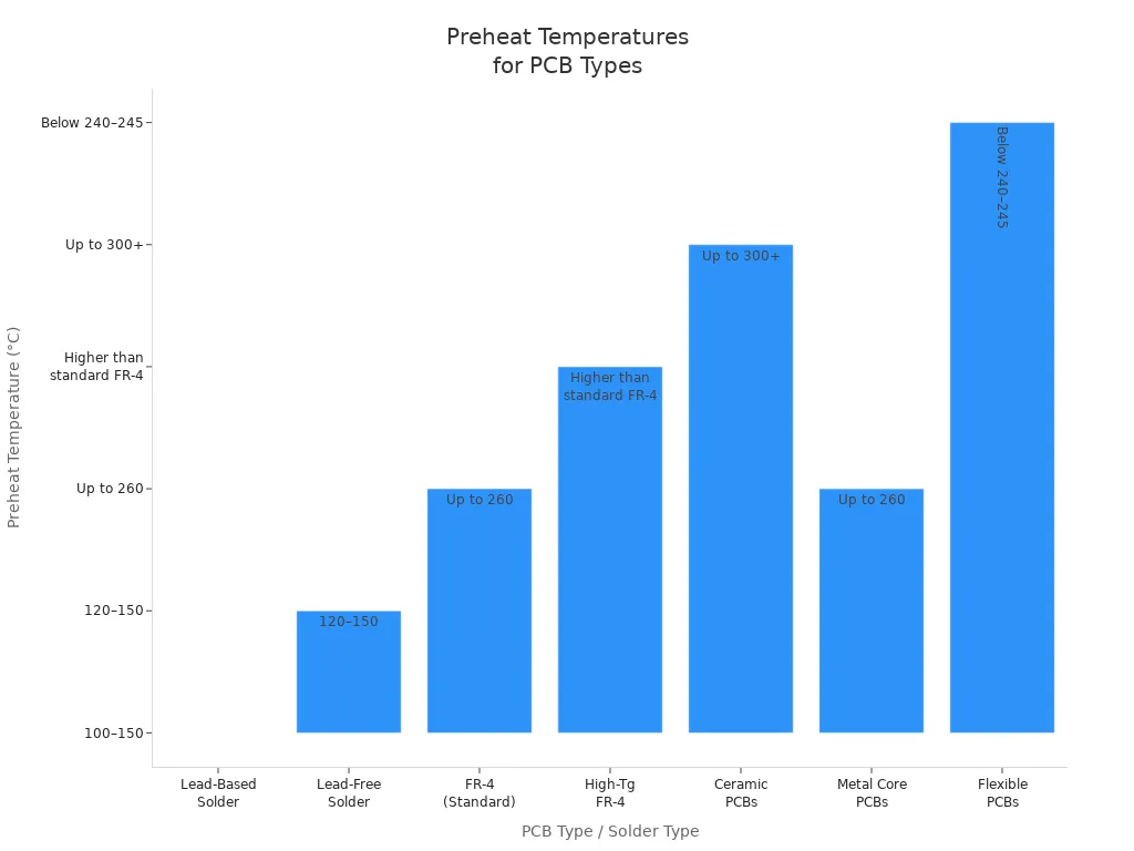
You can improve wave soldering by carefully managing temperature at every stage. Start with preheating the PCB to activate the flux and remove oxides. For most boards, preheat temperatures range from 100°C to 150°C. The solder pot temperature depends on the solder type: use 240°C to 255°C for lead-based solder and 250°C to 270°C for lead-free solder. Keep the PCB in contact with the solder wave for 2 to 5 seconds. Cooling should be gradual to avoid thermal shock.
|
Parameter |
Recommended Range |
|---|---|
|
Preheat Temperature |
|
|
Solder Pot Temperature |
240–270°C (type-dependent) |
|
Soldering Time |
2–5 seconds |
|
Cooling Slope |
5–12°C per second |
If you set the temperature too low, solder may not melt completely, causing cold solder joints. Too high, and you risk damaging components or the PCB. Use thermal profiling tools to monitor and adjust your process. Testing with dummy boards helps you find the best settings for each PCB type.

Wetting Angle
The wetting angle shows how well solder spreads on the pad and component leads. A small angle (less than 30°) means good wetting and strong joints. A large angle (above 90°) signals poor wetting and weak connections. You can control the wetting angle by keeping surfaces clean, using active flux, and setting the right temperature and conveyor speed. Good wetting reduces cold solder joints and boosts reliability.
-
Small wetting angle = strong, even joints
-
Large wetting angle = weak, incomplete joints
-
Clean surfaces and proper flux help maintain a low wetting angle
Surface Tension
Surface tension controls how solder flows and forms joints. When you manage surface tension, you prevent defects like solder bridging and joint tips. Lowering surface tension—by adjusting temperature or using protective oil at the wave crest—helps solder flow evenly and stick to pads. Matching the PCB exit speed to the wave speed gives surface tension time to pull excess solder back, leaving clean, reliable joints. Using these techniques, you can improve wave soldering quality and reduce rework.
Equipment Maintenance

Cleaning Procedures
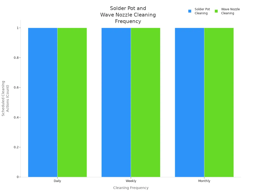
You can Improve Wave Soldering quality by following a strict cleaning schedule for your equipment. Daily cleaning of the solder pot and wave nozzles removes dross and prevents contamination. Dross forms when molten solder meets oxygen, creating oxides that lower solder quality. You should power off and cool the machine before cleaning. Remove solder dross from the pot, use reducing powder to minimize buildup, and clean nozzles with lint-free cloths and proper solvents. Weekly maintenance includes ultrasonic cleaning of nozzles, lubricating pump bearings, and inspecting sensors. Monthly deep cleaning involves removing old lubricants, calibrating soldering parameters, and checking mechanical components. This routine keeps your equipment in top condition and reduces defects.
|
Frequency |
Solder Pot Cleaning |
Wave Nozzle Cleaning |
Additional Notes |
|---|---|---|---|
|
Daily |
Remove solder dross from the solder pot surface; add reducing powder to minimize buildup |
Clean flux nozzles and solder wave nozzles to prevent blockages and residue buildup |
Use lint-free cloths and appropriate solvents; ensure equipment is powered off and cooled before cleaning |
|
Weekly |
Clean wave soldering components, including nozzles, pumps, and motor,s to remove residue and old lubricants |
Ultrasonic cleaning of flux nozzles and cleaning of solder wave module nozzles; lubricate solder pump bearings |
Inspect and clean flux spray modules and PCB sensors; check solder wave stability |
|
Monthly |
Deep cleanthe solder pump and motor; remove dross and old lubricant |
Clean flux nozzles thoroughly; inspect and replace nozzle seals if damaged |
Calibrate soldering parameters; inspect mechanical components and cooling fans |
A manufacturer who adopted daily dross removal and weekly preventive maintenance saw the first pass yield jump from 85% to 96% in three months. Regular cleaning also reduces cold joints and bridging defects.

Oxidation Prevention
Oxidation is a major cause of soldering defects. You can minimize oxidation by using nitrogen knives or creating an inert atmosphere around the solder pot. Nitrogen displaces oxygen, which lowers oxidation and improves solder spread. This leads to stronger, cleaner joints and fewer defects like bridging or incomplete fills. Nitrogen also stabilizes solder temperature and preserves flux activity. Studies show that using nitrogen can reduce PCB rework by up to 75%. Cleaner joints mean higher reliability and less rework.
|
Measurable Improvement |
Description / Impact on Solder Joint Quality |
|---|---|
|
Nitrogen creates an inert atmosphere that stabilizes solder temperature, enhancing wetting on metal surfaces. |
|
|
Reduced Solder Defects |
Minimizes oxidation-related defects such as non-wetting and dewetting, leading to fewer joint failures. |
|
Stronger Mechanical Joints |
Cleaner joints with less oxidation result in improved mechanical strength and reliability. |
|
Cleaner and Stronger Joints |
Reduced flux oxidation preserves flux activity, producing cleaner solder joints. |
|
Enhanced Process Consistency |
Nitrogen use leads to repeatable and reliable soldering results, improving overall process stability. |
|
Lower Rework Rates and Higher Yields |
Fewer defects and stronger joints reduce the need for rework and increase production efficiency. |
Tip: Always monitor your equipment for signs of oxidation and schedule regular maintenance. Clean equipment and a controlled atmosphere help you achieve consistent, high-quality solder joints.
Solder and Flux
Material Selection
Choosing the right solder and flux is one of the most important steps you can take to improve wave soldering quality. You should always match the flux type to your cleaning process and reliability needs. For example, rosin-based flux works well but needs cleaning after soldering. No-clean flux leaves little residue and usually does not require cleaning. Water-soluble flux is highly active and easy to clean, making it a good choice for high-reliability assemblies.
-
Select a flux that matches your solder alloy and process (lead-free or leaded).
-
Apply flux precisely to avoid excess residue, which can cause corrosion or electrical problems.
-
Store flux in sealed containers at room temperature, away from air, moisture, and heat.
-
Use fresh flux for rework to improve wetting and oxidation removal.
Tip: Always follow the manufacturer’s cleaning recommendations for your chosen flux. This helps prevent long-term reliability issues.
The acidity of your flux directly affects how well it removes oxides from metal surfaces. Stronger acids clean faster and improve solderability, but they can leave behind residues that may cause corrosion or electrical failures, especially in humid environments. You need to balance flux strength to get good wetting without risking long-term problems.
Solder Quality
High-quality solder alloys make a big difference in reducing defects. Lead-free solders, which have more tin, oxidize faster and can form more defects if not handled properly. Using a nitrogen atmosphere in the solder tank helps limit oxidation and improves solder flow. This reduces problems like bridging and incomplete joints.
Maintaining the right solder temperature is also key. If the temperature is too low, solder may not wet the pads and leads, causing weak joints. If it is too high, you risk damaging components or the PCB. Clean solder and flux reduce the chance of joint failures and improve reliability.
|
Solder/Flux Criteria |
Why It Matters |
|---|---|
|
Proper flux type |
Ensures easy cleaning and reliability |
|
Compatible solder alloy |
Reduces oxidation and defects |
|
Clean, fresh materials |
Lowers the risk of joint failures |
|
Correct temperature control |
Prevents weak or damaged joints |
When you choose the right materials and keep them clean, you set yourself up for fewer defects and stronger, more reliable solder joints.
PCB Design
Component Alignment
You can improve wave soldering quality by paying close attention to component alignment. Proper alignment ensures that solder flows evenly and covers all pins. Use precise placement tools, such as pick-and-place machines, to achieve accuracy within ±0.1 mm for fine-pitch parts. Always double-check alignment before soldering, especially on smooth surfaces, to prevent components from sliding out of place. Pre-tin component leads before insertion to help solder flow and reduce heat exposure.
When you orient components in the same direction as the solder wave, you help all pins get soldered at the same time. Place large connectors so their pins travel perpendicular to the wave. This prevents trailing pins from missing solder. Avoid putting small components behind larger ones in the wave direction. Large parts can block the solder wave, causing shadowing and poor joints on smaller parts.
-
Use clear polarity markings for accurate orientation.
-
Maintain at least 125 mils between components and the board edge.
-
Space surface mount parts away from through-hole pins to avoid blocking solder flow.
-
Align multi-pin parts with the wave direction to prevent shadowing.
Tip: Shimming or raising connectors helps keep tall or uneven components at the right height, ensuring the solder wave reaches every pin.
Footprint and Clearance
Optimizing footprints and clearances on your PCB reduces soldering defects. Proper pad and solder mask design control how much solder flows and where it goes. If you use too much solder paste or misalign pads, you risk solder bridges. Too little solder leads to weak joints or open circuits.
Follow these best practices for footprint and clearance:
-
Keep a minimum solder dam (solder mask clearance) of 4 mils between pads to prevent bridging.
-
Maintain at least 1.6 mils between pad edges and solder mask.
-
Use solder mask bridges between pins that are 4 to 8 mils wide.
-
Control PCB warpage to less than 0.75% of board length for even solder contact.
A well-optimized PCB layout ensures smooth solder flow and reduces common defects like bridging, cold joints, and open circuits. When you follow IPC standards for pad size and spacing, you help prevent shorts and improve overall assembly reliability.
Note: Collaborate with your PCB assembly provider to confirm that your design matches their wave soldering equipment and process requirements.
Improve Wave Soldering Inspection

Visual Checks
You can spot most wave soldering defects by performing careful visual checks. High-quality solder joints have several clear indicators:
-
Even solder flow around both the component lead and the PCB pad
-
No gaps, voids, or bare spots
-
Strong joints that hold components firmly
Use magnification tools such as magnifying glasses, microscopes, or visual cameras to get a closer look at each joint. These tools help you see small defects like unsoldered joints, solder balls, or bridges that you might miss with the naked eye. For boards with fewer components, manual inspection with magnification increases your accuracy and reliability. Automated Optical Inspection (AOI) systems can check up to 95% of surface defects, including solder bridging and lifted components. Some advanced AOI systems, like the Landrex Optima III SSI, inspect PCBs right after wave soldering and generate detailed reports for quick rework.
Tip: Always check for smooth, shiny, and concave solder joints. Use magnification to catch hidden problems early.
Quality Control
A strong quality control process helps you Improve Wave Soldering results and ensures long-term reliability. Start with an incoming inspection to prevent oxidation and storage issues. Use AOI and X-ray machines before and after soldering to catch defects like insufficient solder or voids. Functional testing finds electrical problems that visual checks might miss.
You should also use statistical methods to monitor your process. Traditional tools like Design of Experiments (DoE) and regression models help you tune parameters. Advanced methods, such as Self-Organizing Maps (SOM), analyze large amounts of process data and visualize optimal conditions. These approaches let you respond quickly to production changes and keep your process stable.
-
Maintain daily equipment cleaning and calibration
-
Document all process steps and inspection results
-
Train operators to recognize and fix defects
-
Use real-time monitoring to prevent thermal stress
By combining visual checks, automated inspection, and robust quality control, you reduce defects and extend the life of your assemblies.
You can Improve Wave Soldering quality by focusing on process parameters, equipment maintenance, solder and flux selection, PCB design, and inspection. Applying these methods leads to fewer defects and more reliable assemblies. Continuous improvement brings better process control, skilled teams, and fewer touch-ups. Ongoing monitoring of soldering parameters helps you catch issues early, stabilize results, and reduce rework.
-
Enhanced solder joint quality
-
Lower defect rates
-
Improved first-pass yield
Keep refining your process and monitoring results to achieve lasting success.
FAQ
What is the most common cause of wave soldering defects?
You often see defects from poor temperature control or dirty equipment. Solder joints fail when you do not clean the solder pot or set the right temperature. Regular maintenance and thermal profiling help you avoid these problems.
How often should you clean wave soldering equipment?
You should clean the solder pot and wave nozzles every day. Weekly, you need to inspect and clean pumps and sensors. Monthly, perform deep cleaning and calibration.
Tip: Consistent cleaning keeps your solder joints strong.
Can you use lead-free solder in any wave soldering machine?
Most modern machines support lead-free solder. You must check the temperature range and compatibility of your equipment. Lead-free solder needs higher temperatures, so verify your machine’s specifications before switching.
What does a good solder joint look like?
A good solder joint appears smooth, shiny, and concave. You should see even coverage around the pad and lead.
|
Feature |
Good Joint |
Bad Joint |
|---|---|---|
|
Appearance |
Shiny |
Dull |
|
Shape |
Concave |
Flat |
|
Coverage |
Even |
Uneven |
