
Why Lead-Free Wave Soldering Breaks the Rules Your Line Was Tuned By
There is a recurring production problem: a plant switches its wave-soldering pot from Sn63/Pb37 to SAC305, keeps every machine setting unchanged, and then discovers cold joints, insufficient hole fill, or excessive dross.
The problem is not usually operator error. It is physics—and arithmetic.
Sn63/Pb37 is a eutectic alloy that melts at 183°C. SAC305 (Sn-3.0Ag-0.5Cu) melts at approximately 217°C to 220°C, according to alloy suppliers such as Indium and MacDermid Alpha. That 34°C to 37°C increase is not merely a higher number on the display. Every additional degree of liquidus margin consumed by a higher pot temperature comes out of the usable process window available for preheat, dwell, flux activation, wave contact, and cooling.
Here is a practical comparison:
| Factor | Leaded Sn63/Pb37 | Lead-free SAC305 |
|—|—|—|
| Melting point | 183°C | 217°C to 220°C |
| Typical published pot range | Approximately 243°C to 260°C | Approximately 255°C to 265°C |
| Working margin above liquidus | Approximately 60°C to 77°C | Approximately 35°C to 48°C |
| Wetting behavior | Fast and forgiving | Slower and more sensitive to flux and preheat |
| Oxide-management burden | Low | High; dross forms readily |
| Profile transfer from another alloy | Not applicable | Rarely works as a direct copy |
This is why lead-free profiles are not directly transferable from leaded lines. The working window is narrower, and there is no single lead-free profile that works for every board.
A line running 1.6 mm FR4 with large through-hole connectors is very different from one running four-layer boards with heavy ground planes and fine-pitch footprints. The correct settings depend on board thermal mass, component mix, board finish, flux chemistry, and the specific alloy in the pot. Generic numbers produce generic—and often incorrect—results.
This guide provides manufacturer-published starting ranges for common lead-free alloys, a step-by-step tuning workflow, and a defect-to-parameter troubleshooting map for production teams. It is framed for high-volume SMT production, where most lead-free conversions are taking place in 2026.
Published: 26 October 2026
Reading Time: 12 minutes
Reviewer: [Reviewer Name, TBD, S&M Co. Ltd. Process Engineering Team]
Why Lead-Free Wave Soldering Breaks the Rules Your Line Was Tuned By
Here is a scene I hear almost every week on the support side of the business: a plant switches its wave solder pot from Sn63/Pb37 to SAC305, keeps every setting on the machine exactly where it was, and then wonders why the board looks fine at the end of the conveyor but fails inspection. Cold joints. Insufficient hole fill. Dross piling up in the pot overnight.
The problem is not operator error. It is physics, and it is arithmetic.
Sn63/Pb37 is a eutectic alloy that melts at 183°C. SAC305 (Sn-3.0Ag-0.5Cu) melts somewhere around 217°C to 220°C, a 34 to 37°C jump, according to alloy suppliers like Indium and MacDermid Alpha. That is not just a higher number on the display. Every degree of extra liquidus margin you spend on a higher pot temperature comes straight out of the usable process window you have left for everything else: preheat, dwell, flux activation, wave contact, and cooling.
Here is the comparison in plain terms.
| Factor | Leaded Sn63/Pb37 | Lead-free SAC305 |
|—|—|—|
| Melting point | 183°C | 217°C to 220°C |
| Typical published pot range | About 243°C to 260°C | About 255°C to 265°C |
| Working margin above liquidus | Roughly 60°C to 77°C | Roughly 35°C to 48°C |
| Wetting behavior | Fast, forgiving | Slower, more sensitive to flux and preheat |
| Oxide management burden | Low | High, dross forms readily |
| Profile transfer from the other alloy | Not applicable | Rarely works as a straight copy |
So when someone says lead-free profiles are not transferable from leaded lines, they are right, and the reason is the narrowing of that window.
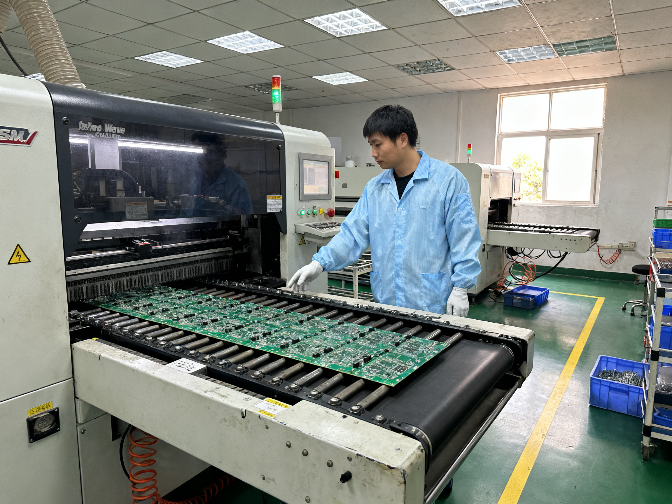
And here is the part that gets missed: there is no single lead-free profile either. A line running 1.6 mm FR4 with a few large through-hole connectors behaves nothing like a line running four-layer boards with heavy ground planes and fine-pitch footprints. The right settings depend on board thermal mass, component mix, board finish, flux chemistry, and the specific alloy in the pot. Hand one plant a generic set of numbers and you get one generic answer, and it will be wrong somewhere.
This guide is built to avoid that. It gives manufacturer-published starting ranges for common lead-free alloys, a step-by-step tuning workflow, and a defect-to-parameter troubleshooting map you can actually work from at the machine. Everything is framed for high-volume SMT production, which is where most of these conversions are happening right now in 2026.
Written by [Author Name, TBD], S&M Co. Ltd. / Shenzhen Chuxin Electronic Equipment Co., Ltd.] [Author Name] works directly with S&M’s wave soldering and reflow equipment lines, supporting manufacturers in consumer electronics, semiconductor, automotive, and military electronics production. Their hands-on work with lead-free profile qualification, dross reduction, and BGA/QFN defect troubleshooting informs every recommendation in this guide. Full author credentials and product-line references will be added at publication, pending confirmation.## About the Author
Written by [Author Name, TBD], S&M Co. Ltd. / Shenzhen Chuxin Electronic Equipment Co., Ltd.]
S&M is the international brand of Shenzhen Chuxin Electronic Equipment Co., Ltd., a Shenzhen manufacturer founded in 2000. The company builds lead-free reflow ovens, wave soldering machines, selective wave equipment, conveyors, loaders, buffers, curing ovens, stencil printers, and full SMT lines for consumer electronics, semiconductor, automotive, military, and aerospace customers. You can see the equipment range on the S&M company site.
The author works directly with S&M’s wave soldering and reflow equipment lines. Day-to-day work includes lead-free profile qualification, dross troubleshooting, and BGA/QFN defect analysis on high-volume production lines.
Every range and troubleshooting step in this guide comes from that hands-on work plus published alloy and process data from suppliers and standards bodies.
Full author credentials, role title, and product-line references will be added at publication, pending internal confirmation.## 1. The Alloy Decision That Sets Your Entire Temperature Window
Most people treat the alloy choice as a purchasing decision. You order SAC305 because it is the industry default, your customer spec says SAC305, the pot gets filled. Then you start tuning. But the alloy actually sets your temperature profile before a single machine parameter is touched.
Here is why. Every wave solder profile is a chain: pot temperature, preheat ramp and soak, wave contact, then cooling. Change the alloy and you change the melting point, the wetting speed, the copper dissolution rate, and the amount of oxide your pot produces. Change any one of those and every setpoint downstream shifts.
First, a correction that matters more than it sounds. SAC305 is Sn-3.0Ag-0.5Cu, meaning 96.5% tin with 3.0% silver and 0.5% copper. It is sometimes described loosely as Sn99/Cu0.5/Ag0.5, which is wrong, and the difference matters when you read a supplier certificate.
Here is how the common alloys compare. Liquidus figures come from published supplier data, including Indium’s alloy listings and AIM’s SAC305 technical data sheet.
| Alloy | Composition | Liquidus | Wetting behavior | Dross tendency | Typical pot temperature | Best fit |
|—|—|—|—|—|—|—|
| SAC305 | Sn-3.0Ag-0.5Cu | 217°C to 220°C | Slower than SnPb, sensitive to flux activity and preheat | High, and copper pickup raises it further | 255°C to 265°C | General purpose lead-free, most automotive and industrial specs |
| SAC405 | Sn-4.0Ag-0.5Cu | Roughly 217°C to 220°C | Very similar to SAC305 | High | 255°C to 265°C | Same process window as SAC305, marginally different mechanical behavior |
| SAC305 plus extra silver | Vendor specific | Varies by certificate | Generally comparable | Varies, no controlled universal data | Confirm with supplier | Only when a drawing or approved materials list names it |
| SN100C | Sn, 0.7% Cu, 0.05% Ni, trace Ge | Eutectic at 227°C | Good flow, small additions stabilize the bath | Lower than SAC in the field | Around 250°C to 260°C | Low-silver programs with copper-dissolution concerns |
Note the SAC405 row. MACDermid Alpha publishes essentially the same melting interval as SAC305, so moving to 4% silver does not buy you a different generic pot setpoint. If someone tells you SAC405 needs its own recipe, ask them to show you the data.
Now the part that confuses people most. Liquidus is not your target temperature. It is the point where the last grain of solid disappears, and your pot needs to sit well above it to keep the wave flowing and to feed heat into the joint. But the ceiling on that pot temperature is set by something else entirely: the package.
A 0402 resistor can sit through thermal abuse. A QFN with a large exposed pad under a heavy ground plane on a four-layer board cannot. When you push a board that already carries a lot of heat into the wave, the component body sees a temperature that no supplier datasheet agreed to. That is where delamination, bond lifting, and die lifting come from, and it is why the “component body limit” is the real constraint on your lead-free wave solder temperature profile rather than the alloy’s melting point.
The widely quoted 260°C figure comes from IPC/JEDEC J-STD-020’s reflow classification table, which assigns peak temperatures by package thickness and volume. Some small packages get classified at 260°C, while thicker or larger ones get 250°C or 245°C. That is a reflow classification, not a wave soldering mandate, and the number your process is actually held to is the lowest limit from the contract, the drawing, the approved materials list, or the part datasheet.
One more myth to clear out. There is a common belief that adding silver reduces dross. It is repeated often enough that it sounds like fact. Direct controlled evidence was not located to support it. Kester does report that hotter solder and greater agitation both increase dross, that lead-free can generate roughly twice the dross of SnPb, and that nitrogen blanketing cuts it sharply. But silver content was not isolated as the driver. So do not pick an alloy for dross reasons without your own pot data.
Choose the alloy from your contract and your board mix, then tune the profile to that alloy. Copying a profile across alloys is where most of the wasted shift hours come from.
Looking ahead, the next section covers preheat and flux, which is where the narrower lead-free window really bites.
Reviewer Note: This section was reviewed against supplier-published data from Indium, AIM, MacDermid Alpha, Kester, and Nihon Superior, with publication rules on alloy composition and pot ranges applied per AIM’s wave soldering profile supplement. Author and reviewer credentials remain placeholders pending internal confirmation.## 2. The Four Zones of a Lead-Free Wave Solder Profile: Pot, Preheat, Wave, and Cooling
A lead-free wave solder profile is not one temperature. It is four zones chained together, and each one steals thermal budget from the next. Get the order right and the numbers stop fighting each other.
Here is the chain: the pot holds the solder, the preheat zone brings the board and its flux up to temperature, the wave forms a moving contact with the bottom of the board, then the assembly cools. Every parameter below lives inside one of those four buckets.
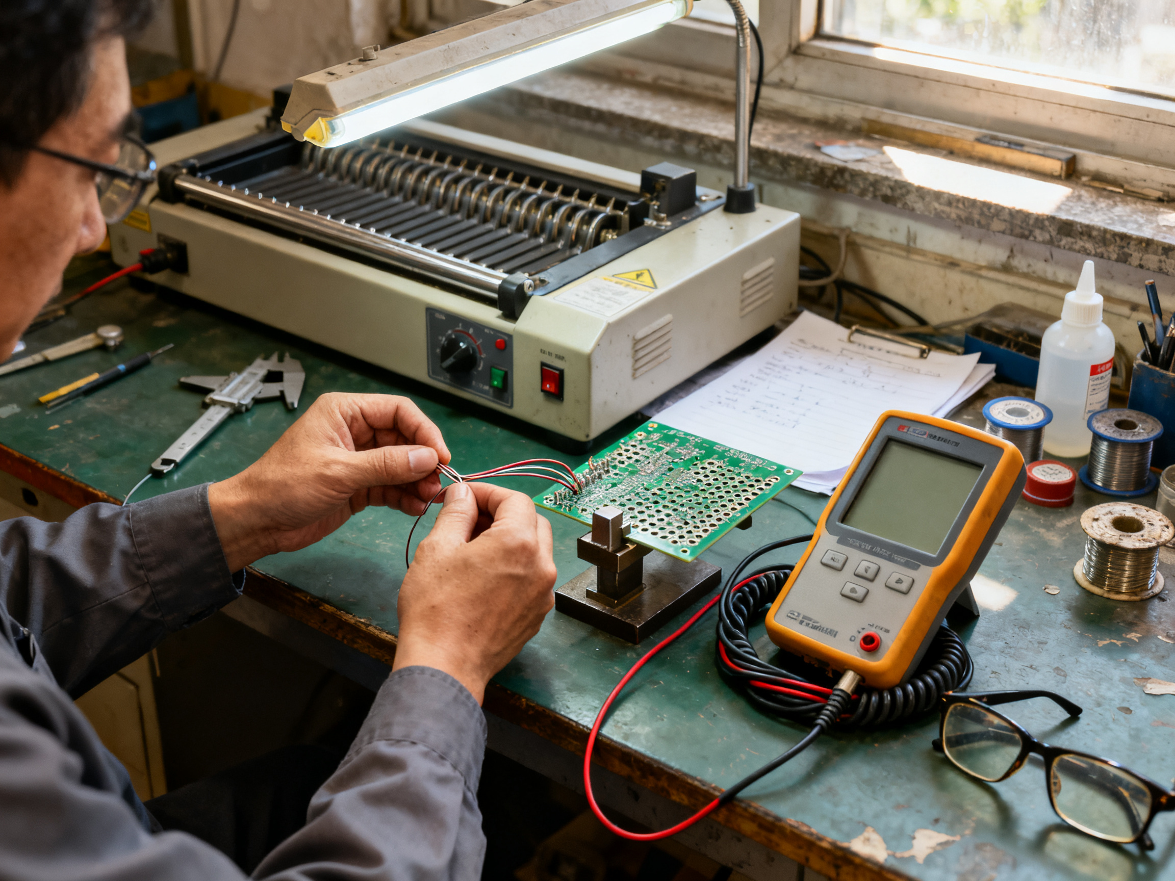
Zone 1: The solder pot
For SAC305, the strongest manufacturer starting range is 255°C to 265°C, which is what MacDermid Alpha and Kester publish for wave soldering of SAC305 and SAC405 alloys. AIM’s broader development guidance runs higher, roughly 255°C to 300°C, and that spread is not an error. It reflects a real spread in machine design, board family and flux chemistry.
The pot has to sit above liquidus (217°C to 220°C for SAC305) so the wave flows and feeds heat into the joint. The ceiling comes from your lowest component or material limit, not from the alloy. If a drawing or datasheet caps a package at 250°C, then 255°C is already over budget.
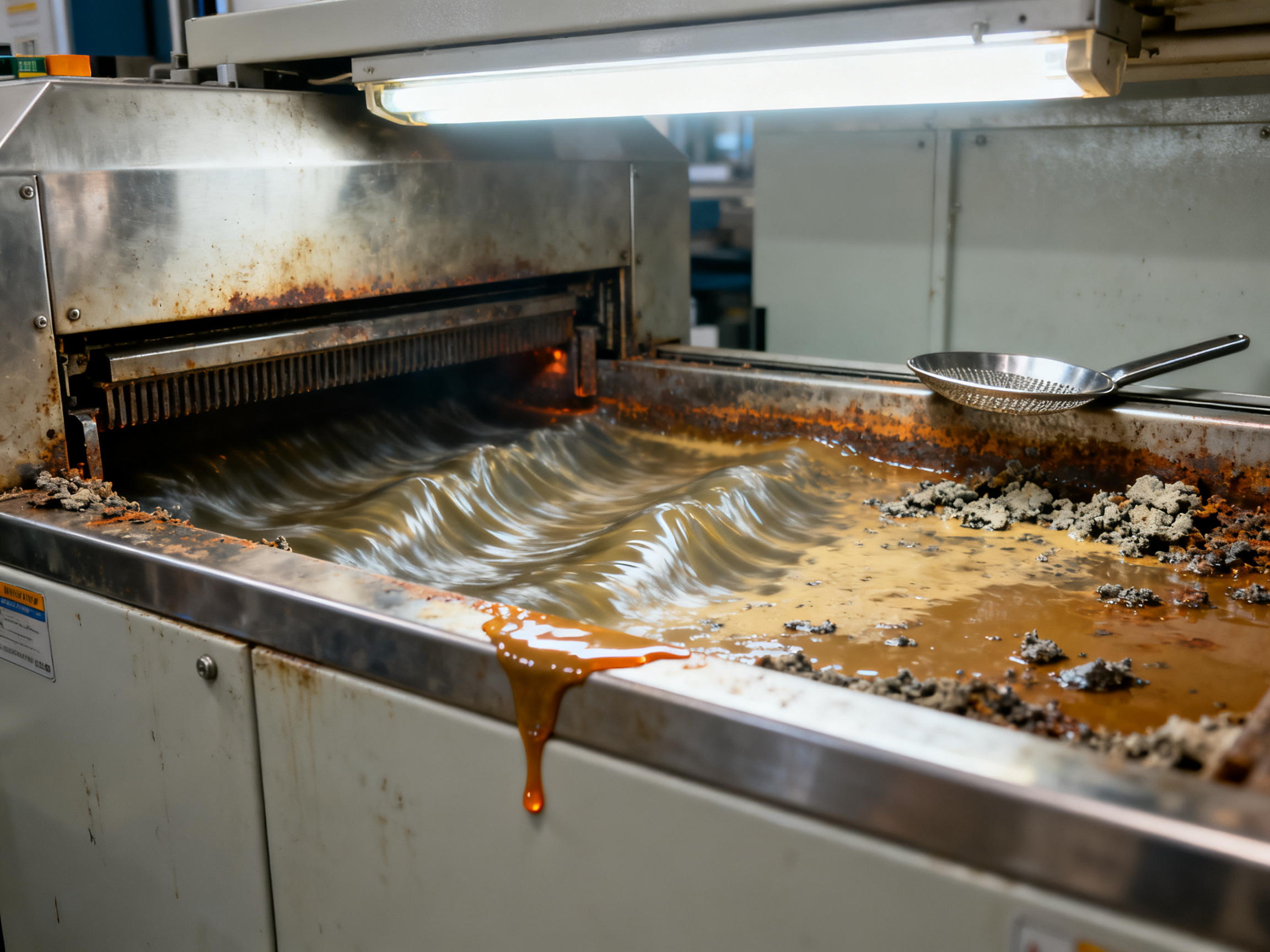
Zone 2: Preheat and soak
This is where lead-free hurts most, because the alloy needs more heat to wet and the flux has less margin to work in.
AIM’s published starting range for lead-free is 80°C to 140°C top-side preheat, a ramp of 1°C to 3°C per second, and roughly 60 to 180 seconds of conditioning from about 40°C up to wave contact. Many production teams target a measured board temperature near 130°C to 160°C for dense or mixed-technology boards, with 60 to 120 seconds of soak, so the board arrives at the wave hot and even.
Two practical notes. First, measure the board, not the air. A Kester validation study recorded top-side preheat around 129°C to 131°C on the board, while another published example used a 93°C to 102°C flux preheat zone, so the setpoint number and the real board number are not the same thing. Second, the soak exists to equalize temperature across the board. A four-layer board with heavy ground planes and a 0402 resistor on the same panel are thermal strangers. Extend the soak before you raise the pot.
Zone 3: The wave
Three parameters matter here, and one of them is not a pot temperature.
| Wave parameter | Starting range for SAC305 | Note |
|—|—|—|
| Wave contact time | 2.3 to 2.8 seconds, single wave | 3.0 to 3.5 seconds for dual wave |
| Conveyor or drag speed | 1.0 to 1.5 m/min | AIM advises keeping bottom-side contact under 5 to 8 seconds |
| Wave height | Often set as one-half to two-thirds of board thickness | Roughly 1.5 to 2.5 mm on typical 1.6 mm boards |
| Drag speed for rework and selective work | 1.0 to 2.5 m/min common on bench machines | Machine-specific, verify on your own rig |
Track the wave crest temperature separately from the pot setpoint. They drift, especially once the pot is loaded with copper pickup. And notice how many sources express wave height as a fraction of board thickness rather than in millimeters. That is the more portable way to carry a recipe to a new machine.
Zone 4: Cooling
There is no universal wave-solder cooling rate, and no published standard says cool to a specific temperature within a specific time. What you do need is a cooling profile that does not move the joint, shock the package or warp the board.
In practice, teams aim to bring the assembly down toward 100°C or below before it leaves the conveyor, then handle flux residue per the flux supplier’s cleaning guidance. Residual flux plus heat encourages tin whisker growth in lead-free alloys, so residue control is not cosmetic. It is a reliability control.
One last framing note, because it saves arguments later. Manufacturer starting range, measured board temperature, and your qualified production window are three different things. AIM’s own wave soldering profile supplement keeps them separate on purpose, and so should your process documentation.
Coming up next: the tuning workflow that turns these starting points into a recipe you can actually run.
Reviewer Note: Zone ranges in this section were checked against supplier-published wave soldering data from MacDermid Alpha, Kester, and AIM, including Kester’s contract-assembly validation study. Published ranges are starting points and require board-, flux-, and machine-specific qualification before production use.## 3. Recommended Temperature Ranges by Application and Board Type
Now the part where most lines get into trouble. A plant asks for the lead-free wave solder temperature profile, and gets one number for the pot. Then they run a smartphone board in the morning and a thick automotive ECU in the afternoon, and the same recipe fails on both.
The alloy window is shared. The rest is not.
Pro Insight: A “one number for the pot” recipe fails on mixed boards because the pot only pays for the liquidus gap. Everything else, preheat, soak, wave contact, cooling, is spent on thermal equalization and flux work. Read the four zones as one thermal budget, not four independent setpoints. If the preheat is short, the pot absorbs the difference and your component bodies pay for it in delamination risk.
Here is the reference table. The alloy throughout is SAC305 unless noted, and every value is a starting range that still needs qualification on your own machine, flux, and board.
| Application | Pot temp | Top-side preheat and soak | Wave contact | Drag speed | Notes |
|—|—|—|—|—|—|
| Consumer electronics, high volume | 255°C to 265°C | 100°C to 140°C, 60 to 120 seconds | 2.3 to 2.8 seconds, single wave | 1.2 to 1.5 m/min | Cost-driven, tightest control on speed and dross rather than peak heat |
| Semiconductor packaging and sub-assembly | 255°C to 265°C | 120°C to 140°C, 90 to 180 seconds | 2.3 to 2.8 seconds, single wave | 1.0 to 1.5 m/min | High mix, fine pitch, so soak and flux deposit vary panel to panel |
| Automotive | 255°C to 265°C | 110°C to 140°C, 90 to 180 seconds | 2.5 to 3.0 seconds | 1.0 to 1.2 m/min | Traceability and long dwell matter more than cycle time |
| Military and aerospace | 255°C to 265°C, or SN100C at 250°C to 260°C | 120°C to 150°C, 120 to 180 seconds | 2.5 to 3.0 seconds, single wave, minimal | 1.0 to 1.2 m/min | Thermally heavy boards, hermetic parts, tightest component limits |
Where those numbers come from matters as much as the numbers themselves. AIM publishes lead-free starting guidance of roughly 255°C to 300°C pot, 80°C to 140°C top-side preheat, a 1°C to 3°C per second ramp, and about 60 to 180 seconds of conditioning from around 40°C to wave contact, with bottom-side contact kept under 5 to 8 seconds, per its wave soldering profile supplement. MacDermid Alpha and Kester publish the tighter 255°C to 265°C window with 1.0 to 1.5 m/min conveyor speed and 2.3 to 2.8 seconds single-wave contact. Those are different machines, different fluxes, and different board families, so the spread is real.
What board thermal mass changes
Here is the rule I would put on the wall of the wave area. Heavy boards do not get a hotter pot. They get a hotter and longer preheat.
A multilayer board with heavy ground planes, a thick-copper power module, or a metal-core assembly arrives at the wave with a cold core and a warm surface. If you cannot equalize that in the preheat zone, the wave does the equalizing for you, and it does it by dumping heat into the joint and the component body at the same time. IPC’s lead-free implementation material notes that large temperature differentials may need longer soak zones and sometimes longer time above liquidus.
So the adjustment order is fixed. Extend soak first, then re-measure the coldest ground-connected through-hole and the hottest component body, then adjust the pot within the alloy supplier window, and only then look at wave contact time.
The hard limits you cannot negotiate
Three limits cap everything above.
Component body temperature. The number your process is held to is the lowest of the datasheet, the contract, the drawing, and the customer addendum. The famous 260°C figure comes from IPC/JEDEC J-STD-020’s moisture and reflow sensitivity classification table, and it varies by package thickness and volume. Thin, small packages can be classified at 260°C. Larger or thicker ones land at 250°C or 245°C. That is a reflow classification, not a wave soldering rule, and it is not a target to aim for. It is a ceiling.
Ramp-up rate. AIM’s 1°C to 3°C per second guidance exists because faster ramps drive outgassing and thermal stress, not because a faster ramp saves meaningful time. A 20-second conveyor zone still has to do its job.
Time above liquidus and total exposure. Bottom-side contact stays below 5 to 8 seconds, and total time above liquidus stays bounded. Long exposure buys nothing in a lead-free process, it only adds package stress.
Cooling gets less attention than it deserves, and there is no published universal wave cooling rate to lean on. What you do need is a ramp that does not move the joint, shock a ceramic part, or warp a long panel. Bring the assembly down toward 100°C or below before it leaves the conveyor, then handle residue per the flux supplier’s guidance. Residual flux plus heat encourages tin whisker growth in lead-free alloys, so residue control is a reliability control, not housekeeping.
For a quick visual of what a qualified lead-free profile should look like across the four zones, use this as your reference chart and overlay your own thermocouple traces:
LEAD-FREE WAVE SOLDER PROFILE (SAC305)

  °C
 265 ┤            ┌──── Wave crest 255-265°C
 250 ┤            │     ╭──╮  contact 2.3-2.8 s
 240 ┤            │    ╱    ╲
 220 ┤            │   ╱      ╲
 200 ┤            │  ╱        ╲
 180 ┤            │ ╱          ╲
 160 ┤         ╭──╯             ╲
 140 ┤        ╱  Preheat 100-140°C
 120 ┤      ╱    soak 60-180 s
 100 ┤    ╱
  80 ┤  ╱
  60 ┤╱
  40 ┤
     └──┴──────┴──────────────┴──→
      Ramp   Preheat   Wave    Cooling
      1-3°C/s  Soak    Contact
The next section walks through the tuning workflow that turns these starting ranges into a recipe you can sign off on. If you want to see how these zones map onto real hardware in the meantime, S&M’s wave soldering equipment range covers both inline and selective configurations built for lead-free pots.