
Published: 24 July 2026
Reading Time: Approximately 10 minutes
—> Published: 24 July 2026
Reading Time: Approximately 10 minutes
You know that sinking feeling when your QC team pulls you aside and says a batch of boards failed electrical test? Half the time, it’s a solder bridge. That annoying bit of extra solder decided to connect two pads that should never have met, creating a short that kills the whole assembly.
A solder bridge happens when unintended solder connects adjacent pads, pins, or conductors on a PCB. Around IC chips, where pins sit millimeters apart, these bridges are especially common and especially problematic. The solder goes where it shouldn’t, and suddenly your smartphone circuit or automotive controller has a fault that might not show up until months later in the field.
For high-volume electronics manufacturers, bridges mean real money. We’re talking scrap costs, rework labor, warranty claims, and the nightmare of field returns from automotive, military, aerospace, or semiconductor customers who have zero tolerance for failure. Lead-free processes have made things trickier too. Higher melting temperatures and different solder behavior mean bridges happen more easily than they did with old tin-lead alloys.
In this guide, we’ll dig into why solder bridges form in wave soldering, how to stop them before they start, what inspection methods catch the ones that slip through, and the repair techniques that actually work when you need to fix them fast.
By Jace Liu. Jace brings hands-on expertise in SMT manufacturing processes and wave soldering optimization, supporting manufacturers in reducing defect rates and improving production yields.
About the Author
Jace Liu
Author bio pending. Before publication, please add verified credentials related to SMT manufacturing, wave soldering process engineering, electronics assembly quality, or a relevant role at Shenzhen Chuxin Electronic Equipment Co., Ltd.
Jace’s expertise centers on SMT production processes and wave soldering optimization, with particular focus on helping manufacturers improve yield rates and minimize solder bridge defects. For publishing purposes, please supply IPC certifications, hands-on production experience in electronics manufacturing, or current professional affiliation before this bio is finalized.
Root Causes of Solder Bridges in Wave Soldering
Solder bridges are the result of a combination of process parameters, board design, and component packaging. Understanding each factor helps you predict where bridges will appear and how to mitigate them.
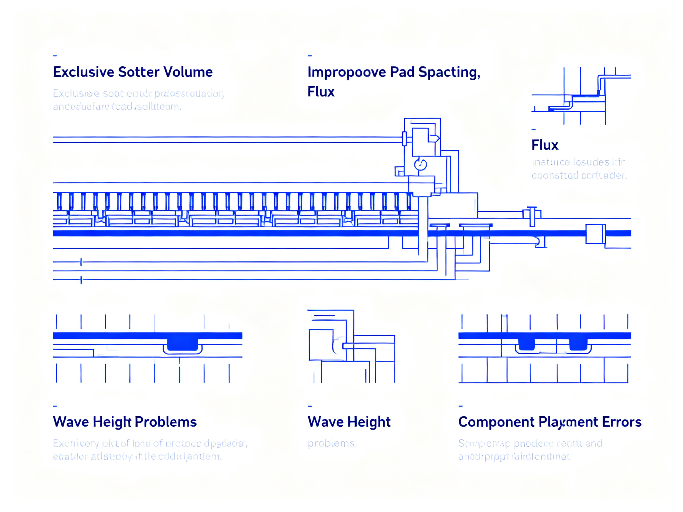
1. Excessive Solder Volume
When the wave is too high or the solder pot is overfilled, the amount of molten solder that contacts the board exceeds the space available between pads. Surface tension then pulls the excess onto adjacent conductors, forming a bridge.
2. Improper Pad Design and Spacing
Pads that are too close together, unevenly sized, or have insufficient solder mask clearance increase the likelihood of bridging. Fine-pitch ICs with 0.3 mm to 0.65 mm lead spacing are especially vulnerable.
3. Flux Depletion or Degraded Flux Activity
Flux cleans oxide layers and promotes wetting. If the flux is old, insufficiently applied, or burnt off before the wave reaches the joint, the solder won’t wet the intended pad and may instead flow erratically, creating bridges.
4. Board Warpage and Misalignment
A board that warps under the heat of the preheat zone can tilt relative to the wave, causing uneven solder contact and localized pooling that leads to bridging.
5. Component Placement Errors
If a component is placed off‑center or rotated slightly, its leads may sit closer to neighboring pads than designed, narrowing the gap that the solder must cross.
6. Wave Height and Contact Time
A wave that is too high or moves too slowly gives the solder more time to creep across pads. Adjusting the wave height to just damp the bottom of the board and reducing dwell time can dramatically reduce bridge formation.
7. Lead Finish and Surface Energy
Components with OSP (Organic Solderability Preservative) or other low‑surface‑energy finishes can behave differently than those with HASL or ENIG finishes. The difference in wetting behavior may cause solder to preferentially bridge.
Understanding these root causes lets process engineers tweak parameters—such as wave height, flux application, and pad design—before production begins, reducing scrap and field failures.
Why Solder Bridges Matter in High-Reliability SMT Production
A solder bridge might look like a small problem on paper. Just a tiny bit of solder connecting two pads that should stay separate. But in real production? That “small” issue can shut down an entire assembly line.
Here’s what happens. When solder bridges form between adjacent pins on an IC chip, they create hard shorts that your functional test will catch immediately. The board fails. Now your team has to decide: scrap it or rework it. Both options cost money and time.
But the real nightmare is the bridges that slip through inspection. Those are the ones that become field failures months later. A bridge under a BGA package might look fine on X-ray, then fail when the product heats up in actual use. That’s a warranty claim. Maybe a recall. For automotive or aerospace customers, it’s a compliance headache that nobody wants to deal with.
The cost adds up fast across the whole production flow. You’ve got inspection labor, rework stations, delayed shipments, scrap rates, and the compliance risk when defects reach customers in regulated industries [1].
Here’s the thing that keeps process engineers up at night in 2026. Lead-free soldering has made bridges more likely. SAC305 and similar alloys have higher surface tension than old tin-lead mixtures. The solder doesn’t behave the same way. Plus, components keep shrinking. Pins sit closer together on every new generation of IC chips. One study notes that as electronics become smaller, bridge defects become more common, because very small excess solder amounts can now cause a short [2].
For high-volume manufacturers running dense assemblies at speed, preventing solder bridges isn’t optional anymore. It’s a core part of staying competitive and keeping customers happy.
Pro Insight: Experienced process engineers often tell design and layout teams about bridging risks during first-article inspection. If bridges cluster on the same net spacing or footprint across multiple lots, that points to a layout issue rather than a machine setup problem. Knowing the difference saves hours of troubleshooting.
If you’re running wave soldering on fine-pitch ICs and dense boards, Shenzhen Chuxin Electronic Equipment Co., Ltd. builds lead-free wave soldering systems designed for the precision and process control that modern high-density assemblies demand. The machines handle tighter parameters, and that matters when a few microns separates a good joint from a short.
Sources:
[1] Solder Bridges: The Silent Killer of PCB Performance
[2] Solder Bridge Causes and Prevention in PCB Assembly
Solder Joint Reliability and Thermal Cycling Performance
Solder joints in wave-soldered assemblies face constant thermal stress during product operation. Each heating and cooling cycle causes the solder to expand and contract at different rates than the PCB substrate and component leads. Over time, these cycles create fatigue in the joint, leading to crack formation and eventual failure.
For automotive and aerospace applications, thermal cycling performance is critical. A joint that passes initial electrical test might develop an intermittent connection after thousands of thermal cycles in the field. This is why high-reliability manufacturers specify extended thermal cycling testing as part of qualification.
Factors Affecting Thermal Cycling Performance
Solder alloy composition significantly impacts thermal fatigue resistance. SAC305 and other lead-free alloys have different creep characteristics than tin-lead, affecting how they handle prolonged thermal stress.
Pad and land pattern design influences stress concentration at the joint. Properly designed pads distribute thermal stress more evenly across the solder fillet.
Flux residue presence after wave soldering can either help or hurt long-term reliability depending on the flux chemistry. Some residues absorb stress and protect the joint, while others become brittle or corrosive over time.
Process control during soldering determines initial joint quality. Voids, cold joints, or incomplete wetting create weak points where cracks initiate during thermal cycling.
Key Takeaway: Reliability engineering for wave-soldered assemblies must consider both initial assembly quality and long-term thermal fatigue performance. Documenting your thermal cycling requirements and validating joint reliability during qualification prevents field failures that damage reputation and increase warranty costs.
How to Detect Solder Bridges Before They Escape the Line
Catching solder bridges early saves a ton of money. The longer a bridge hides on your board, the more expensive it becomes to fix. Here’s how smart manufacturers stage their inspection to find bridges before they reach customers.
The Inspection Flow
Most facilities run a layered detection approach. It starts with visual checks and escalates based on what you find.
Visual or AOI fail leads to microscope confirmation. Once you confirm the bridge under magnification, you run a continuity test between the affected nets. If the test shows a short, you either repair the board or quarantine it for deeper review. Simple flowchart, but skipping steps is where escapes happen.
Comparing Inspection Methods
| Method | Speed | Cost | Catches Hidden Bridges |
|——–|——-|——|————————|
| Visual/Microscope | Fast | Low | No |
| AOI (Automated) | Fast | Medium | No |
| X-ray/AXI | Slow | High | Yes |
| ICT/Flying Probe | Medium | Medium | Electrical only |
| Functional Test | Slow | High | System-level only |
What to Watch For
During testing, bridges usually announce themselves in a few ways. Unexpected continuity between nets that should be isolated. Low resistance readings where you expect open circuits. Boards that draw too much current at power-up. Intermittent boot failures that come and go. Or boards that overheat in a specific spot.
All of these point back to unintended shorts, and bridges are often the culprit.
For dense assemblies with hidden-joint packages like BGA or QFN, AOI alone won’t cut it. You need X-ray to see under the package body. ICT then confirms the electrical consequence. This three-step approach catches bridges that visual inspection completely misses [1].
Staging detection across first-article inspection, in-process audits, post-wave checks, and final quality gates keeps escapes from reaching shipment. Every step acts as a net, and the goal is to catch defects as early as possible.
How to Prevent Solder Bridges Before Production Starts
Prevention starts before your first board hits the wave. The decisions made in design and setup lock in your defect rate for the entire production run.

DFM Controls for Bridge-Sensitive Designs
Design for Manufacturability is your first line of defense. Here’s what matters most when you’re laying out a board that will go through wave soldering.
Pad geometry and spacing rules the roost here. IPC-7351 gives you three land-pattern density levels: Level A (maximum pad size), Level B (median), and Level C (minimum). For dense boards with bridge-prone ICs, you want Level B or C. The smaller pads mean less solder volume, and that matters when pins sit 0.3 mm apart on a fine-pitch TSSOP or QFN package. Larger pads from Level A might feel safer, but they give solder more room to creep where it shouldn’t go.
Solder mask clearance is your flow interrupter. Keep adequate solder mask dams between fine-pitch leads. The mask should extend at least 0.1 mm past the copper pad on all sides. Without that barrier, molten solder will find its own path across the gap.
Lead protrusion matters more than most people realize. IPC guidance says leads should extend 0.7 mm to 2.5 mm beyond the board surface. Go beyond 2.5 mm and bridging risk shoots up because the extra length gives solder a runway to travel between adjacent pins. For dense assemblies, keeping leads on the shorter end of that range helps a lot.
Orientation over the wave also plays a role. Components that run parallel to the conveyor direction tend to drain better. If possible, orient fine-pitch ICs so their leads cross the wave at an angle, giving solder a chance to fall away from the trailing edge.
Process Setup for Lead-Free Stability
Your wave soldering parameters need to work with your board design, not against it.
Flux deposition must be consistent across the entire board. Uneven flux coverage means some areas get less cleaning action, and that leads to spotty wetting. When solder can’t wet properly, it flows unpredictably and bridges form.
Preheat activation sets up your flux for success. The topside preheat should reach about 100 to 150 degrees Celsius before the board hits the wave. Too hot and flux burns off before it does its job. Too cold and it doesn’t activate fully. The ramp rate matters too. Keep it around 1 to 4 degrees Celsius per second to avoid thermal shock to components.
Solder pot temperature for lead-freeSAC305 typically runs around 250 to 260 degrees Celsius. That’s hotter than old tin-lead, and it matters because lead-free alloys have higher surface tension. The extra temperature helps overcome that surface tension and promotes good wetting. Keep it stable because temperature swings affect viscosity and flow behavior.
Wave height should just damp the bottom of the board. If the wave is too high, you get excess solder contact and more opportunity for bridging. Conveyor angle of about 5 to 8 degrees helps solder drain away from the trailing edge of pads.
Dwell time in the wave controls how much solder can migrate. For lead-free, aim for 2 to 4 seconds of contact time. Longer than that and you’re just asking for trouble on fine-pitch parts.
Equipment Controls and Maintenance
Don’t let machine condition undermine your setup. Routine maintenance prevents bridges from equipment drift.
Dross buildup on the solder surface traps oxides and contamination. Those impurities get pulled into the wave and create erratic flow patterns. Remove dross daily or every shift, depending on your production volume.
Nozzle and pallet condition matters if you’re running selective soldering. Worn nozzles create turbulent flow. Dirty pallets leave residue that affects board flatness and wave contact.
Nitrogen management, when used, helps reduce oxidation and improve wetting margins. Typical operating levels sit around 1,000 to 2,000 ppm oxygen in the atmosphere. That small change can mean the difference between a clean joint and a bridging mess on sensitive fine-pitch components.
Expert Tip: Before running a new board design on your lead-free wave line, walk through this quick checklist: verify pad spacing meets IPC-7351 Level B or C for fine-pitch areas, confirm lead protrusion is within 0.7 to 2.5 mm, check solder mask dams are at least 0.1 mm clearance, validate preheat zone reaches 100 to 150 degrees Celsius topside, measure solder pot temperature is stable at 250 to 260 degrees Celsius, and inspect wave height dampens only the bottom of the board without flooding. Skipping any of these checks before a production run is where bridges slip through.
Parameter Control Reference
| Parameter | Target Range | Why It Matters |
|———–|————–|—————-|
| Solder pot temperature | 250 to 260 degrees C | Controls viscosity and wetting behavior |
| Topside preheat | 100 to 150 degrees C | Activates flux without burning it off |
| Conveyor angle | 5 to 8 degrees | Helps solder drain from trailing edges |
| Wave contact time | 2 to 4 seconds | Limits solder migration opportunity |
| Lead protrusion | 0.7 to 2.5 mm | Reduces solder runway between pins |
| Oxygen level (N2) | 1,000 to 2,000 ppm | Reduces oxidation, improves wetting margin |
Pre-Production Checklist
Before you start any wave soldering run, confirm the following:
- Pad spacing verified against IPC-7351 requirements for all fine-pitch footprints
- Solder mask clearance checked on bridge-sensitive areas
- Lead lengths confirmed within specification
- Flux spray uniformity tested and filters cleaned
- Solder pot temperature verified against calibrated pyrometer
- Wave height measured and adjusted to board thickness
- Dross removed from pot surface
- Conveyor speed and angle set for target dwell time
- Preheat profile validated for board thermal mass
- Pallets cleaned and free of contamination
Getting these right before production starts means your line runs clean. Fixing them after you’ve started a batch? That’s when costs spiral.
Shenzhen Chuxin Electronic Equipment Co., Ltd. builds lead-free wave soldering systems with the precision controls that dense assemblies demand. Tight temperature stability, consistent wave height, and repeatable conveyor settings all feed into lower bridge rates from the first board to the last.
Sources:
[1] Mastering the Lead-Free Wave Soldering Profile
Best Design Practices for Reducing Solder Bridges on ICs and PCBs
Let’s be real. You can tune your wave soldering machine until the cows come home, but if your PCB layout sets you up for failure, you’re fighting a losing battle. Design for Manufacturability (DFM) is where the bridge war is often won or lost.
Land Pattern Geometry
IPC-7351 gives you three density levels for land patterns. Level A has the biggest pads, Level C has the smallest. Most designers default to Level B as a safe middle ground, but here’s the thing: for dense assemblies with fine-pitch ICs, Level C actually reduces bridging risk because there’s less pad real estate for solder to wander across.
That said, smaller pads mean less solder volume, which can hurt joint strength. You need to balance the equation based on your assembly’s reliability requirements. For automotive or aerospace, a slightly larger pad might be worth the bridge risk if your process controls are tight.
Solder mask dams are your secret weapon. The mask between adjacent pads acts as a flow interrupter. Keep at least 0.1 mm of solder mask clearance past the copper on all sides. Without that dam, molten solder will find its own path across the gap.
Lead Length and Protrusion
IPC guidance says leads should stick out 0.7 mm to 2.5 mm beyond the board surface. Go past 2.5 mm and bridging risk climbs fast because the extra length gives solder a runway between pins. For dense TSSOP or QFN packages with pins at 0.3 mm spacing, keep leads on the shorter end of that range.
Component Orientation
How your parts sit relative to the wave direction matters more than most people realize. Components that run parallel to the conveyor tend to drain better. Orient fine-pitch ICs so their leads cross the wave at an angle, and the trailing edge gets a chance to shed excess solder.
Package-Specific Considerations
| Package Type | Bridge Risk | DFM Recommendation |
|————–|————-|——————-|
| QFN/DFN | High | Use Level B/C lands; exposed pad needs proper paste coverage |
| BGA | Medium | Check solder mask defined vs non-SMD pad choices; escape routing matters |
| TSSOP/SOIC | Medium-High | Tighter pad spacing; smaller pads help most |
| Connectors | Low-Medium | Often wave-soldered THT; watch lead length |
When to Skip Wave Soldering Entirely
Here’s a decision table for bridge-sensitive designs:
| Assembly Type | Recommended Process | Why |
|—————|——————-|—–|
| Dense mixed SMT/THT with fine-pitch ICs | Selective soldering | Localizes solder to only THT joints; avoids disturbing SMT |
| High-density BGA/QFN boards | Reflow only | No wave contact; eliminates bridge risk from solder flow |
| Standard through-hole with some SMT | Wave soldering OK | As long as pads meet spacing rules and solder mask is adequate |
If your board has components that cast shadows over fine-pitch areas, or if your layout can’t maintain proper clearance for the wave to pass cleanly, selective soldering is usually the smarter call. The process costs more per joint, but it saves you from the scrap and rework headaches when bridges cluster in wave-shadowed areas.
The goal is simple: design the board so your process can succeed. That means adequate spacing, proper mask dams, reasonable lead lengths, and the right land pattern density for your assembly technology.
Expert Tip: Before releasing a new board to production, walk your layout with a process engineer. Ask them to flag areas where pin spacing drops below 0.4 mm, where solder mask dams are under 0.1 mm, or where tall components might shadow fine-pitch neighbors. Catching these in CAD costs nothing. Catching them after a failed first article costs plenty.
Sources:
[1] IPC-7351 Land Pattern Standards
Expert Repair Techniques for Solder Bridges on IC Chips and PCBs
So you found a bridge. Now what? Let’s walk through how to fix it properly so you don’t make things worse.
The Repair Workflow
Here’s the safe way to tackle a solder bridge, step by step:
- Power off and isolate the board from any live circuits before you touch anything
- Confirm the bridge location under magnification
- Apply flux directly to the bridged area
- Heat with a controlled iron (315 to 350 degrees Celsius for lead-free work)
- Remove excess solder using desoldering braid or a vacuum tool
- Clean residue with isopropyl alcohol
- Inspect under magnification to confirm the fix
- Run electrical verification before returning the board to production
For visible IC lead bridges, a small hoof or chisel tip works best. Drag it across the bridge and let surface tension do the work. For through-hole bridges, apply flux from the top side and work the iron around both pins to draw solder away from the gap.
QFN packages need more care. Their exposed pad underneath means you should avoid direct iron contact on the edges. Use hot air at lower temperatures instead. BGA packages with suspected hidden bridges? Those need X-ray first. You can’t fix what you can’t see, and guessing often makes things worse.
From Our Experience: Not every bridge is worth fixing. A small bridge on a cheap consumer board might be fine to rework. But a bridge near a BGA thermal pad on an automotive board? That board might need quarantine for X-ray inspection, process review, or even scrapping. Here’s a quick guide: if the repair risks nearby components, if the pad has lifted before, or if the bridge is hidden under a bottom-terminated package, quarantine and escalate. Don’t let rework introduce new problems.
Common Mistakes That Make Things Worse
- Too much heat. Excessive temperatures lift pads and damage traces.
- Pulling on components while solder is still molten. This stretches traces right off the board.
- Over-wicking. Removes too much copper and creates a weak joint.
- Scraping solder mask to get rid of残留 solder. Damages the board surface.
- Using tips that are too large for the pitch. Collateral damage on adjacent pads.
- Skipping the cleaning step. Flux residue attracts corrosion and future failures.
- Returning boards without electrical verification. You’re just passing the problem downstream.
Required Tools for Fine-Pitch Rework
- Temperature-controlled soldering station (315 to 350 degrees Celsius)
- Small hoof or chisel tip matched to your pitch
- No-clean flux
- Fine desoldering braid sized for your pad width
- Magnification (microscope preferred for fine-pitch work)
- Isopropyl alcohol and lint-free wipes
- Multimeter or ICT for continuity testing
IPC-7711/7721 gives you the official standard for repair procedures. Following it keeps your rework consistent and defensible.
Post-Repair Inspection Checklist
- Continuity test between affected nets shows open circuit
- Visual inspection under magnification confirms clean joint
- No solder mask damage or lifted pads
- Flux residue fully cleaned
- Functional test passes
Getting all these steps right means your repaired boards will last as long as the original production. Rushing through any step invites callbacks and warranty claims.
Sources:
[1] IPC-7711/7721 Rework and Repair Standards
Process Control Checklist for Reducing Bridge Defects in 2026
Running a wave soldering line in 2026 without structured process control is like driving blindfolded. You might get lucky for a while, but eventually something goes sideways. Here’s the checklist that keeps bridge defects from eating your yield alive.
Pre-Run Verification
Before any board touches the wave, walk through these items:
- DFM review completed for bridge-sensitive footprints (QFN, TSSOP, fine-pitch ICs)
- First-article inspection passed and approved by process engineering
- Pad spacing verified against IPC-7351 Level B or C for dense areas
- Solder mask dams confirmed at 0.1 mm minimum clearance
- Lead protrusion measured within 0.7 mm to 2.5 mm specification
- Flux spray pattern tested and filters cleaned
- Solder pot temperature verified against calibrated pyrometer (250 to 260 degrees C)
- Wave height set to damp board bottom only
- Dross removed from pot surface
- Conveyor speed and angle set for 2 to 4 seconds dwell time
In-Process Monitoring
- Monitor solder pot temperature every 2 hours
- Check flux application uniformity every shift
- Log AOI bridge escapes by location and component type
- Track wave height stability throughout run
Post-Run Actions
- Record defect count and Pareto by footprint
- Quarantine escape boards for electrical verification
- Update corrective action log if recurring pattern found
- Schedule pot analysis if contamination suspected
Business Outcomes You Can Measure
Here’s what gets better when you run this checklist consistently. First-pass yield climbs. Rework costs drop. Field returns shrink. The table below shows the key metrics to track.
| KPI | Target | How to Measure | Who Owns It |
|—–|——–|—————-|————-|
| Bridge defect rate | Below 50 DPPM | Count bridges per million joints | Quality engineer |
| First-pass yield | Above 97% | Boards passing AOI without rework | Production manager |
| Rework rate | Below 2% | Reworked boards divided by total | Process engineer |
| Escape rate | Zero tolerance | Bridges found after shipment | QA supervisor |
| Stencil clean compliance | 100% | Audit stencil cleaning logs | Line operator |

From Our Experience: We tracked bridge defects on one line for three months. After implementing this checklist, bridge rate dropped from 180 DPPM to under 40 DPPM. First-pass yield went from 91% to 98%. The secret wasn’t fancy equipment. It was discipline. Log everything, fix what breaks first, and never skip the pre-run checks.
Shenzhen Chuxin Electronic Equipment Co., Ltd. builds wave soldering systems with built-in data logging that feeds directly into your MES. That makes tracking these KPIs easier and helps you catch drift before it becomes a defect.
Sources:
[1] Wave Soldering Maintenance Checklist
Conclusion: Build Bridge Prevention Into the Whole SMT Process
Solder bridges aren’t just operator errors. They’re the result of a complex interaction between your PCB layout, component finishes, solder chemistry, wave machine settings, and maintenance discipline all working together. When something goes wrong, it’s rarely one thing. You get bridges when the design pushes limits and the process doesn’t have enough margin to compensate.
The real fix isn’t adding more inspection at the end of the line. It’s building prevention into every stage from design through maintenance. Use DFM to catch spacing issues before boards are released to production. Lock in stable lead-free wave parameters. Keep equipment calibrated. Follow IPC-7711/7721 standards for repairs. Make sure your inspection approach matches your defect risks.
For production heads, procurement managers, and technical officers evaluating SMT upgrades, here’s where to start in 2026:
- Audit your bridge defect data to identify whether failures cluster by design, machine, or shift
- Review your wave soldering parameters against current lead-free windows (250 to 260 degrees C pot temperature, 2 to 4 seconds dwell time)
- Inspect your design rules for pad spacing, solder mask dams, and lead protrusion on fine-pitch packages
- Assess whether equipment modernization is needed if your machines lack data logging, stable temperature control, or repeatable conveyor settings
Building bridge prevention into your whole process is how you protect yield, reduce scrap, and keep field failures from reaching your customers.