Manufacturers often choose wave soldering for high-volume production of through-hole boards because it offers speed and cost savings. Reflow soldering best fits projects with surface-mount components or complex, high-density designs that require precision. The choice depends on several factors:
- Component types on the board
- Required production volume
- Equipment and setup costs
- Desired quality and reliability
Recent market trends show that both methods remain dominant, with Asia-Pacific leading global adoption. Selecting the right process ensures efficient, high-quality assembly.
Key Takeaways
- Wave soldering suits high-volume production with through-hole components, offering fast, cost-effective assembly and strong mechanical joints.
- Reflow soldering excels with surface-mount devices, providing precise, reliable solder joints for complex, high-density boards and supporting lead-free processes.
- Manufacturers often combine both methods on mixed-technology boards to optimize quality and efficiency.
- Choosing the right soldering method depends on component types, board design, production volume, quality needs, and budget constraints.
- Following a clear decision checklist helps reduce defects, ensures compliance, and matches the soldering process to project requirements.
Comparison
Comparison Table
| Performance Metric | Wave Soldering | Reflow Soldering |
| ——————————— | ——————————————————————————————– | —————————————————————————————————— |
| Speed (Production Efficiency) | Batch process; conveyor speed 0.5–2.5 m/min; ideal for high-volume through-hole components | Sequential process; conveyor speed 0.5–1.5 m/min; inline ovens for SMT components |
| Cost (Equipment & Setup) | Equipment cost $20,000–$100,000; includes soldering machine and solder pot | Higher initial cost $50,000–$300,000; includes reflow oven, stencil printer, inspection systems |
| Precision (Quality & Reliability) | Robust joints; risk of bridging and solder balls if not optimized; nitrogen improves quality | High precision for SMT; controlled thermal profiles reduce defects; advanced temperature control |
| Component Compatibility | Best for through-hole components; not suitable for delicate SMT components | Ideal for surface-mount technology; supports miniaturization and fine-pitch components |
| Environmental Impact | Less energy efficient; entire PCB immersed in molten solder; moderate solder waste | More energy-efficient, localized solder paste, supports lead-free alloys, better regulatory compliance |
Key Differences
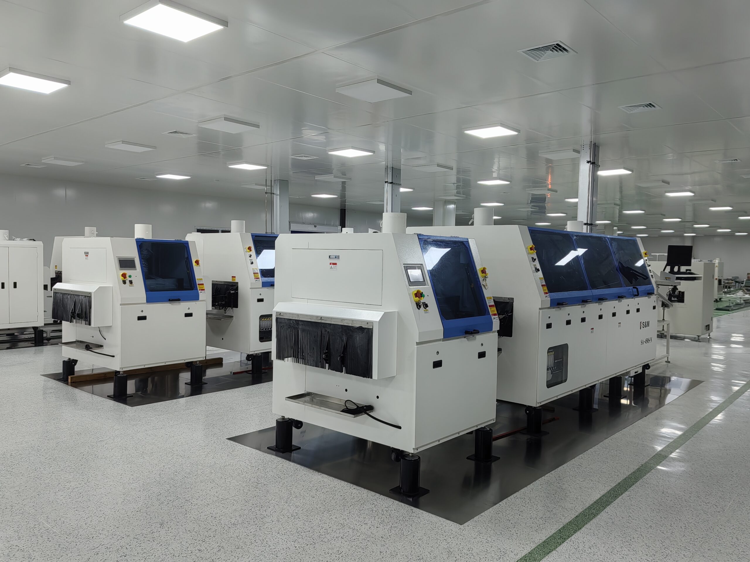
- Wave Soldering works best for through-hole components and high-volume production. It offers fast throughput and lower initial setup costs. However, it uses more energy and creates more solder waste because the entire board passes through molten solder.
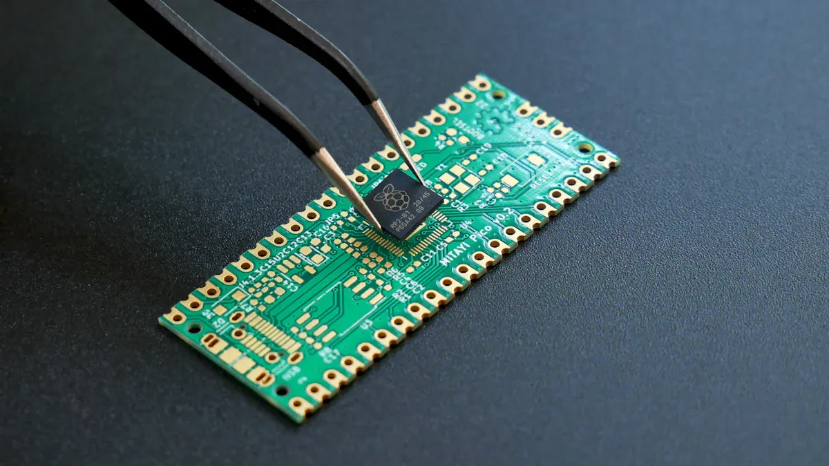
- Reflow soldering excels with surface-mount components, especially on complex or high-density boards. It provides better solder joint quality and reliability due to precise temperature control. The process supports lead-free solder, making it more environmentally friendly. Initial equipment costs are higher, but the method allows for miniaturization and advanced board designs.
- Experts note that reflow soldering uses a controlled heating profile, which reduces defects and supports fine-pitch components. Wave Soldering, on the other hand, requires careful temperature management and is less suitable for delicate parts.
- Manufacturers sometimes combine both methods on a single board. They typically use reflow soldering for SMT parts first, then apply wave soldering for through-hole components. This hybrid approach helps meet the needs of mixed-technology assemblies.
Tip: Choosing the right soldering process depends on the types of components, production volume, and quality requirements. Reviewing these key differences helps manufacturers match their needs to the best method.
Wave Soldering Overview

How It Works
Wave Soldering uses a series of automated steps to join electronic components to printed circuit boards. The process works efficiently for high-volume production and through-hole technology. Here is a typical workflow:
- Flux Application: Operators apply flux to the underside of the PCB using spray or foam methods. This step prevents oxidation and ensures strong solder joints.
- Preheating: The board moves through a preheating zone, reaching temperatures between 90°C and 125°C. Preheating reduces thermal shock and prepares the board for soldering.
- Solder Wave Contact: The PCB passes over a wave of molten solder. The solder wave height and conveyor speed are carefully controlled to ensure proper contact with all pads and leads.
- Cooling and Inspection: After soldering, the board cools and undergoes inspection to check for defects.
This automated process enables manufacturers to solder hundreds of boards per hour. Automation reduces labor costs and increases consistency, making Wave Soldering a cost-effective choice for mass production.
Applications
Wave Soldering is most common in assemblies that use through-hole components. Manufacturers rely on this method for:
- Through-hole technology (THT) boards, where leads pass through holes in the PCB.
- Mixed-technology PCBs, combining THT and surface-mount components. Pallets protect SMT parts during soldering.
- Large-scale manufacturing, such as industrial electronics, automotive electronics, and power equipment, where strong mechanical joints are required.
| Assembly Type | Description |
| —————————– | —————————————————————– |
| Through-hole technology (THT) | Soldering components with leads passing through PCB holes |
| Mixed-technology PCBs | Boards with both THT and SMT components, using protective pallets |
| High-volume manufacturing | Production lines need speed and efficiency |
| Industrial and automotive | Electronics demand reliability and robust connections |
Pros and Cons
Wave Soldering offers several advantages:
- Moderate equipment cost compared to other automated methods
- High throughput, processing hundreds of boards per hour
- Reliable joints for power and mechanical stress applications
- Cost savings from reduced labor and fewer defects
However, some disadvantages exist:
| Disadvantage Category | Description |
| ——————— | —————————————————————————– |
| Precision | Limited for fine-pitch SMT components; risk of damage to heat-sensitive parts |
| Selectivity | Solder bridging and shadowing effects can cause defects |
| Environmental Impact | Use of lead-based solder, flux fumes, and high energy consumption |
Note: Manufacturers must optimize process parameters to minimize defects and environmental impact. Wave Soldering remains a preferred method for THT and high-volume production, but it is less suitable for delicate or complex assemblies.
Reflow Soldering

How It Works
Reflow soldering joins surface-mount components to printed circuit boards with a precise, controlled process. The method uses solder paste and a reflow oven to create strong electrical connections. The process includes several critical steps:
- Solder Paste Application: Technicians apply solder paste to PCB pads using a stencil. Accurate placement ensures reliable joints.
- Component Placement: Automated pick-and-place machines position components onto the solder-paste-coated pads with high precision.
- Preheating: The assembly enters a reflow oven, where gradual heating activates flux and removes oxides.
- Soaking: The temperature holds steady to allow uniform heating and stabilize the solder paste.
- Reflow: The oven raises the temperature above the solder’s melting point. The solder paste liquefies, forming strong bonds between components and pads.
- Cooling: The board cools slowly, solidifying the solder joints and preventing thermal stress.
Careful control of temperature profiles and timing prevents defects such as solder bridging, cold joints, or component damage. Reflow soldering supports advanced PCB designs and ensures high reliability.
Applications
Reflow soldering fits modern electronics manufacturing, especially for surface-mount technology (SMT) assemblies. Manufacturers use this method for:
- High-mix, low-to-medium volume SMT production, where flexibility and precise thermal profiling matter.
- Complex PCB designs with multiple component types and high-density layouts.
- Lead-free PCB production requires careful temperature management.
- Double-sided boards, where components are mounted on both sides.
Reflow soldering handles various SMT package types in a single process. It offers flexibility in design and manufacturing, making it ideal for smartphones, computers, medical devices, and automotive electronics.
Tip: Reflow soldering is less wasteful and easier to monitor than wave soldering. It supports miniaturization and advanced electronics.
Pros and Cons
Pros:
- High precision for small and densely packed SMT components.
- Supports double-sided PCB assembly with proper process control.
- Controlled thermal profiles reduce defects and improve joint reliability.
- Automation enables consistent, high-throughput production.
- Flexible for complex and high-density board designs.
Cons:
- Higher initial equipment and material costs.
- Requires specific stencils and templates for each product.
- Regular maintenance and calibration increase operational complexity.
- Specialized technicians must operate and maintain equipment.
- Improper temperature settings can cause defects and reduce reliability.
| Benefit/Drawback | Description |
| ——————– | ———————————————————————————– |
| Precision | Advanced stencil and printing technologies ensure accurate solder paste deposition. |
| Dual-pass capability | Enables double-sided assembly, but risks re-melting bottom-side components. |
| Quality | Controlled profiles and material science improve reliability. |
| Cost | Equipment, solder paste, and maintenance raise expenses. |
| Speed | Setup and changeover times can slow production for high-mix environments. |
Note: Regular monitoring and maintenance help prevent defects and ensure consistent quality in reflow soldering.
Head-to-Head
Process
| Step | Wave Soldering | Reflow Soldering |
| —————- | —————————————————- | ——————————————————- |
| Flux Application | Flux is sprayed on the PCB before soldering | Flux included in solder paste, applied with a stencil |
| Pre-heating | PCB is heated to activate the flux and prevent shock | PCB heated to remove solvents from solder paste |
| Soldering | PCB passes over the molten solder wave | PCB passes through the reflow oven at a set temperature |
| Cooling | Solder joints solidify as the PCB cools | Solder paste cools and fixes components |
| Equipment | Soldering machine with conveyor and solder wave | Reflow oven, pick-and-place machine, stencils |
| Complexity | Requires expert handling and precise control | Easier to manage, less operator-dependent |
Note: Wave Soldering involves more complex machine setup and operator skill. Reflow soldering uses automated equipment and controlled temperature profiles.
Components
| Soldering Method | Compatible Components | Advantages | Limitations |
| —————- | —————————————– | —————————————— | ————————————————- |
| Wave Soldering | Through-hole parts (connectors, switches) | Fast, cost-effective for large boards | Not suitable for small or delicate SMDs |
| Reflow Soldering | Surface-mount devices (SMDs, microchips) | Precise placement supports miniaturization | Higher setup cost, limited for large through-hole |
- Wave Soldering works best for boards with large connectors and mechanical parts.
- Reflow soldering fits designs with tiny chips and high-density layouts.
- Mixed boards often need both methods for best results.
Speed and Cost
| Aspect | Wave Soldering | Reflow Soldering |
| ———- | ———————————- | ————————————- |
| Production | High throughput, hundreds per hour | Moderate throughput, flexible batches |
| Setup Cost | Lower initial equipment cost | Higher equipment and material costs |
| Changeover | Fast for single product lines | Slower for frequent product changes |
- Manufacturers choose Wave Soldering for mass production and lower costs.
- Reflow soldering suits smaller batches and complex boards, but costs more to set up.
Quality and Reliability
| Aspect | Wave Soldering | Reflow Soldering |
| ——————– | ——————————————- | ———————————————— |
| Solder Joint Quality | Strong joints for mechanical stress | Consistent, precise joints for dense electronics |
| Reliability | Favored in industrial and automotive boards | Preferred for consumer and high-tech devices |
| Defect Risk | Solder bridging, cold joints are possible | Tombstoning, component shifting possible |
- Wave Soldering creates robust connections for power and industrial uses.
- Reflow soldering delivers reliable results for miniaturized and high-density electronics.
- Many automotive and advanced boards use both methods to maximize reliability.
Tip: Manufacturers should match their soldering method to the board design and reliability needs for best results.
Choosing the Right Method
Project Needs
Selecting the right soldering process begins with understanding project requirements. Manufacturers consider component types, board density, and production scale. Surface mount technology (SMT) projects often require reflow soldering for precise placement and high-density layouts. Through-hole technology (THT) boards benefit from Wave Soldering, which handles larger components and supports high-volume production.
| Project Requirement | Wave Soldering | Reflow Soldering |
| ———————— | ———————————- | —————————————– |
| Component Type | Through-hole components (THT) | Surface mount components (SMT) |
| Component Density & Size | Larger, high-power components | High-density, small components (BGA, QFP) |
| Production Scale | Cost-effective for large-scale THT | Favored for mass SMT production |
| Quality Requirements | Good mechanical support | High quality, precise temperature control |
| Automation & Efficiency | Efficient for bulk soldering | Efficient for complex SMT boards |
Manufacturers also evaluate volume, complexity, and turnaround time. Larger production volumes reduce per-unit cost, making Wave Soldering attractive for bulk orders. Projects with complex layouts or mixed technologies may require a hybrid approach.
Board Design
Printed circuit board (PCB) design strongly influences soldering method selection. Reflow soldering excels with double-sided boards and fine-pitch components. It minimizes thermal stress and warping, making it suitable for delicate or thin PCBs. Wave Soldering works best for simpler boards with through-hole parts, but it can cause solder bridging or damage to bottom-side SMT components unless protective measures are used.
| PCB Design Aspect | Preferred Soldering Method | Reasoning |
| ————————— | ——————————– | ——————————————————————- |
| SMT-only design | Reflow | High precision and automation for compact layouts. |
| THT-only design | Wave | Cost-effective for boards with only through-hole parts. |
| Mixed-technology board | Hybrid (Reflow + Selective/Wave) | Reflow for SMT; wave or selective soldering for through-hole parts. |
| Double-sided SMT | Reflow | Safe soldering of both sides with thermal control. |
| High-volume, low-cost | Wave | Fast and efficient for the mass production of THT boards. |
| Fine-pitch ICs or BGAs | Reflow | Accurate soldering with tight thermal control. |
| Prototypes or small runs | Reflow | Flexible for design changes and minimal tooling. |
| Large connectors and relays | Wave or Selective | Strong mechanical joints for power or rugged applications. |
Manufacturers often use reflow soldering first for SMT components, then apply Wave Soldering or selective soldering for through-hole parts on mixed-technology boards.
Budget
Budget plays a key role in process selection. Wave Soldering offers lower initial equipment costs and high throughput, making it ideal for large-scale production. Reflow soldering requires higher investment in ovens, stencils, and inspection systems, but it supports advanced designs and automation.
- Equipment and setup costs for Wave Soldering range from $20,000 to $100,000.
- Reflow soldering equipment can cost between $50,000 and $300,000.
- Maintenance and operator training add to ongoing expenses, especially for reflow soldering.
- Lead-free soldering, required by regulations like RoHS, may increase costs due to higher melting points and equipment upgrades.
Manufacturers must balance upfront investment with long-term efficiency and quality. Projects with tight budgets and high volumes often favor Wave Soldering, while those needing flexibility and precision choose reflow soldering.
Decision Checklist
A practical checklist helps manufacturers match their needs to the best soldering method:
- ✅ Identify component types: Are most parts through-hole or surface mount?
- ✅ Review board layout: Is the design dense, double-sided, or mixed technology?
- ✅ Estimate production volume: Will the project run in bulk or small batches?
- ✅ Assess quality requirements: Does the application demand high reliability or mechanical strength?
- ✅ Consider heat tolerance: Are components sensitive to temperature profiles?
- ✅ Evaluate budget: What are the equipment, setup, and maintenance costs?
- ✅ Plan for regulatory compliance: Will the process use lead-free solder and meet environmental standards?
- ✅ Factor in operator skill: Does the team have experience with the chosen method?
- ✅ Implement quality control: Are inspection and testing systems in place?
- ✅ Avoid common mistakes: Check datasheets, thermal profiles, and stencil designs before starting.
Tip: Manufacturers who follow this checklist reduce the risk of defects and costly rework. They also ensure compliance with industry standards such as IPC-A-610 and IPC-J-STD-001, which guide process control and inspection rigor.
Manufacturers should match their soldering method to project needs.
- For high-volume, through-hole, or mixed boards, efficient and cost-effective processes work best.
- For fine-pitch SMDs or complex, high-density layouts, precise temperature control and reduced solder use are preferred.
The decision checklist helps teams evaluate supplier capabilities and process controls.
Explore guides from ALLPCB and Viasion for deeper insights, or partner with experienced electronics manufacturing services for expert support.
FAQ
What types of boards work best with wave soldering?
Manufacturers use wave soldering for boards with through-hole components. This method suits large connectors, relays, and industrial electronics. It handles high-volume production efficiently.
Can reflow soldering handle double-sided PCBs?
Reflow soldering supports double-sided boards. Technicians use precise temperature control to prevent damage. This process allows placement of surface-mount devices on both sides.
Does wave soldering support lead-free processes?
Wave soldering can use lead-free solder. Operators must adjust temperature settings and equipment. Lead-free alloys require higher melting points, which may increase energy use.
How do manufacturers inspect solder joints after reflow?
Technicians inspect solder joints using automated optical inspection (AOI) systems. These machines detect defects like tombstoning or bridging. AOI improves quality and reduces manual errors.
Which method offers better reliability for fine-pitch components?
Reflow soldering provides better reliability for fine-pitch and miniature components. Controlled heating profiles reduce defects. This method supports advanced electronics and high-density layouts.
