
Published: 19 May 2026
Reading Time: 15 minutes
Why Mastering Reflow Soldering Profiles Matters in SMT Manufacturing
Picture this. You’ve just finished assembling a batch of 500 circuit boards for a client’s smartphone order. Everything looks perfect on the surface. But then, testing reveals that 23 boards have faulty solder joints. Cold joints. Bridging. Maybe even some components that lifted right off the board during testing.
Sound familiar? This nightmare scenario plays out in SMT factories around the world, and the culprit is usually the same: a reflow soldering profile that wasn’t quite right.
Here’s the thing about reflow soldering profiles. They might sound like some technical concept only engineers care about, but these temperature curves literally determine whether your electronics work or fail. A reflow soldering profile meaning is pretty simple. It’s basically a recipe that tells your reflow oven exactly how hot to get, how long to stay there, and how fast to cool down when you’re soldering components onto a board.
Get the recipe wrong and you’ll spend more time fixing defects than actually making products. Get it right and your production line hums along with barely any waste.
In modern SMT manufacturing, precision matters more than ever. Components keep getting smaller. Boards keep getting more complex. A single BGA component might have over 200 tiny solder balls underneath it, each one needing perfect conditions to form a reliable joint. There’s no room for guesswork anymore.
The connection between proper profiles and defect reduction is well documented. When manufacturers take time to optimize their reflow profiles, they typically see significant drops in common issues like bridging, tombstoning, and voiding. Plus, components last longer because controlled cooling reduces thermal stress.
In this guide, we’ll walk through everything you need to know about reflow soldering profiles. We’ll cover what makes lead-free profiles different from traditional ones, how to actually create a profile step by step, and what to do when things go wrong. By the end, you’ll have a clear roadmap for getting your soldering process dialed in.
Let’s get started.
About the Author
Jace Liu has spent over 12 years working directly with SMT manufacturing processes and reflow oven technology. He has helped dozens of electronics manufacturers optimize their soldering workflows and reduce defect rates. When he’s not writing about thermal profiles, you can find him troubleshooting production line challenges in actual factories.
Understanding the Basics: What is a Reflow Soldering Profile?
Think of a reflow soldering profile as a cooking recipe for your circuit boards. Just like you need the right temperature and timing when baking a cake, your SMT oven needs specific instructions to create good solder joints.
A reflow soldering profile meaning is essentially a temperature curve that your oven follows during the soldering process. The oven heats up according to this curve, holds certain temperatures for specific times, and then cools down in a controlled way.
The Four Stages of Every Reflow Profile
Every reflow soldering profile breaks down into four main stages. Each one matters for getting solid, reliable solder joints.
| Stage | What Happens | Typical Temperature Range |
|——-|————–|—————————|
| Preheat | Board warms up gradually to remove moisture | Room temp to 150 degrees C |
| Soak | Flux activates and everything equalizes | 150 to 200 degrees C |
| Reflow | Solder melts and forms joints | 235 to 250 degrees C (peak) |
| Cooldown | Controlled cooling solidifies joints | 250 degrees C down to room temp |
The preheat stage is where you gently warm up the board. You want to raise the temperature slowly, usually around 1 to 3 degrees Celsius per second. Going too fast can crack sensitive components or cause defects. We’ve all seen what happens when you pour cold water into a hot glass. Thermal shock is real.
During the soak stage, the board sits at a steady temperature for a while. This gives the flux in your solder paste time to do its job. Flux cleans the metal surfaces so the solder can stick properly. Most profiles hold this temperature for 60 to 120 seconds.
The reflow stage is where the magic happens. This is when your solder paste melts and flows onto the component leads and pads. Peak temperature here is critical. Too hot and you damage components. Too cool and the solder does not melt fully.
Finally, the cooldown stage brings everything back down to room temperature. Cool too fast and you get stress in the joints. Cool too slow and you might get氧化. The rate matters.
Why Ramp Rates Matter So Much
Here is something many people overlook. The speed at which you move between temperatures, called the ramp rate, affects everything. Ramp too fast and you stress components. Ramp too slow and you risk oxidation problems.
Most lead-free profiles use ramp rates between 1 and 3 degrees per second during heating phases. The cooling phase usually happens at 1 to 4 degrees per second. These numbers are not arbitrary. They come from years of testing what works for typical components and solder pastes.
The real challenge is that different components on the same board might need slightly different conditions. A small resistor and a large BGA chip heat up at different speeds. Your profile needs to balance these needs.
Expert Tip: When setting up your reflow profile, start with the component that has the tightest thermal window. Everything else can usually adapt, but sensitive parts like certain QFN packages or thermal sensors need special attention.
Getting these basics right means fewer headaches later. Poor profiles lead to rework, wasted boards, and production delays. Good profiles mean your line runs smooth and your customers get reliable products.
But here is the thing. Understanding what a reflow soldering profile is only gets you so far. You need to know how lead-free profiles differ from traditional ones, and that is where things get interesting.
Key Differences Between Leaded and Lead-Free Profiles
So here is where things get real. If you have been working with SMT manufacturing for any length of time, you have probably heard people argue about lead-free versus leaded solder. There are valid points on both sides. Let me break down what actually matters for your reflow soldering profile.
The biggest difference comes down to temperature. Lead-free solder needs to get significantly hotter than traditional tin-lead solder to melt properly. This changes everything about how you set up your profile.
Temperature Comparison
| Parameter | Leaded Solder (Sn63/Pb37) | Lead-Free Solder (SAC305) |
|———–|—————————|—————————|
| Melting Point | 183 degrees C | 217-221 degrees C |
| Peak Temperature | 225-235 degrees C | 245-260 degrees C |
| Soak Temperature | 140-170 degrees C | 150-200 degrees C |
| Time Above Liquidus | 30-60 seconds | 60-90 seconds |
| Cooling Rate | 1-4 C/s | 1-4 C/s |
Notice the peak temperature difference. Lead-free solder needs to hit around 245 to 260 degrees Celsius, while traditional leaded solder maxes out closer to 235 degrees. That 20 degree gap might not sound like much, but for heat-sensitive components it is a big deal.
Why Temperature Windows Matter
Here is the tricky part. When you run lead-free profiles at these higher temperatures, you have less wiggle room before something goes wrong. Components can degrade. Boards can warp. But go too cool and your solder joints will be weak or incomplete.
We ran into this issue at a factory I consulted with last year. They were switching from leaded to lead-free for automotive客户 work. Their original leaded profiles had plenty of margin for error. The lead-free profiles? Not so much. Every component on the board needed to handle that extra heat without breaking a sweat.
The soak stage also behaves differently between the two. Lead-free profiles usually need longer soak times to get the flux working properly before reflow. This helps prevent voiding and ensures the solder wets correctly on those sometimes-tricky OSP-coated pads.
Compliance and Your Profile
Look, I get that lead-free sounds like a headache. But in most markets right now, you do not have much choice. The EU RoHS directive, plus similar regulations in Asia and North America, basically require lead-free for most electronics sold commercially. If you are making products for consumer electronics, automotive, or industrial applications, lead-free is not optional anymore.
This means your reflow oven needs to be capable of hitting those higher temperatures consistently. Your thermocouples need to be accurate. Your profile needs to be tight.
One thing that helps: newer lead-free solders like SAC305 (tin-silver-copper) have gotten better over the years. They wet more easily than early lead-free formulations did. But they still demand respect.
Expert Tip: When adapting a thermal profile for lead-free soldering, try to keep your time above 217 degrees C (the lead-free liquidus point) as short as possible while still achieving good wetting. Extended time at peak temperature increases intermetallic compound growth, which can make joints brittle over time.
The Real-World Trade-offs
Leaded solder is simply easier to work with in many ways. Lower temperatures mean less stress on components. Wider process windows mean your profile does not need to be dialed in quite as precisely. Plus, leaded solder forms better-looking joints sometimes, with that characteristic shiny finish.
But lead is toxic. Manufacturing workers do not want exposure to it. Environmental regulations are only getting stricter. If you are still running leaded solder in 2026, you are probably serving a very niche market.
The profile differences matter for your yield rates. A well-tuned lead-free profile can actually match or beat leaded solder in terms of defect rates. It just takes more effort to get there.
We have found that factories which invest time in profiling their lead-free process properly see defect rates drop significantly compared to those just running generic profiles off the internet. The machine matters, but the profile matters more.
What This Means for Your Setup
If you are running both types, you need separate profiles. You cannot just crank up the temperature on a leaded profile and call it good. The entire curve shape needs to account for the different thermal requirements.
Most modern reflow ovens handle both easily. The real work is in developing the right profile for each solder type and your specific board assembly.
Step-by-Step Guide to Creating a Reflow Soldering Profile
Now that we understand the theory behind reflow profiles and the differences between lead-free and leaded options, let’s get into the actual process of creating one. This is where theory meets practice.
Gathering Your Tools
First, you need the right equipment for measuring your thermal profile. Without accurate data, you are basically guessing, and guessing does not work in SMT manufacturing.
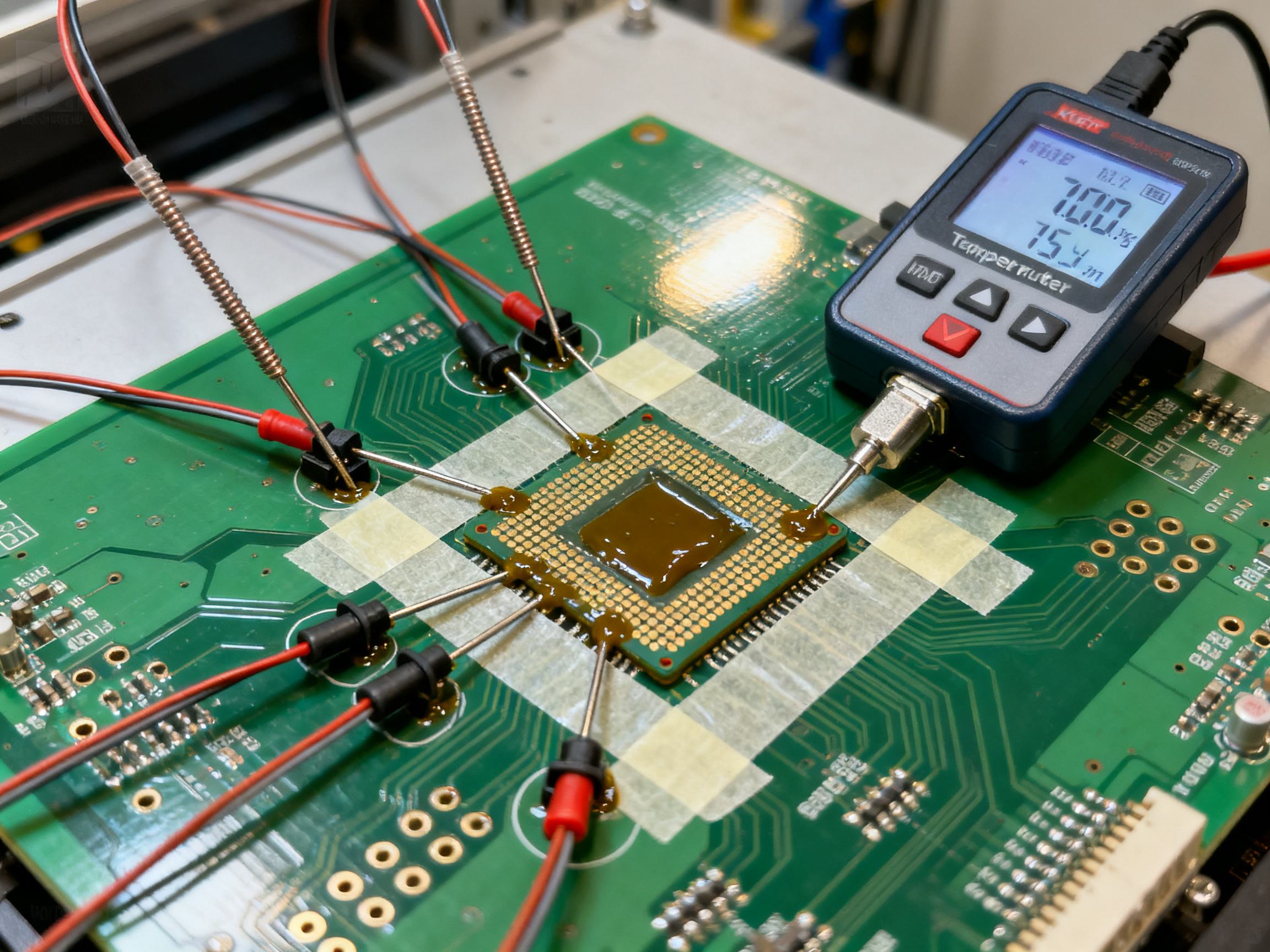
The core tools you need are thermocouples, a data logger, and profile software. Thermocouples are small temperature sensors that attach to your board. They feed real-time temperature data to the data logger during the reflow process.
We use K-type thermocouples most often. They handle the high temperatures involved in lead-free soldering without breaking a sweat. You will need multiple thermocouples, usually 4 to 12 depending on your board complexity. More points mean better data.
The data logger is what records everything. It captures temperature readings at set intervals throughout the entire profile. Most loggers take readings every half-second or faster. You want high resolution so you catch any temperature spikes or dips.
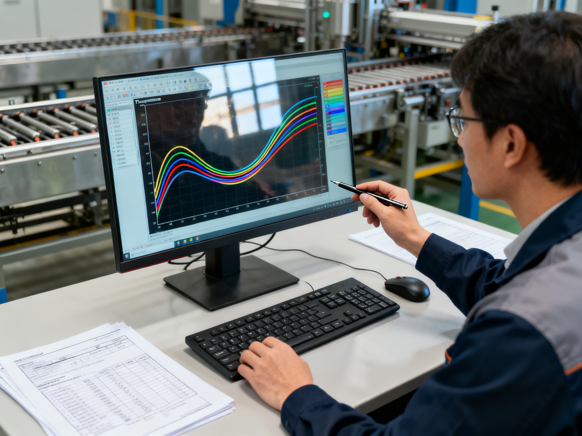
Profile software turns that raw data into visual curves you can analyze. Some software even suggests adjustments based on what it sees.
Preparing Your Board
Before you attach any thermocouples, prepare your test board. It should match your actual production boards as closely as possible. Same size, same components, same solder paste.
Here is a tip that took me a while to learn. Clean your test board before profiling. Any flux residue or contamination can affect heat transfer. You want to measure pure thermal behavior.
Attach your thermocouples to strategic locations. Focus on thermal hotspots and cold spots. For BGA components, put a thermocouple right next to the solder balls. For large connectors, measure both the center and edges. Board thickness and copper weight affect temperatures too, so measure multiple spots.
Secure the thermocouples properly. They need to make good contact with the surface. Use high-temperature tape or adhesive. A loose thermocouple gives you bad data, and bad data leads to bad profiles.
Running Your First Profile
Now run the profile. Load your test board into the reflow oven and execute the profile you want to test. The data logger records everything.
When the cycle finishes, download the data to your profile software. You will see a temperature curve. Compare it against the recommended profile for your solder paste.
Look for several things. Is your peak temperature high enough? Too high? How long does the board stay above the solder melting point? Are your ramp rates within spec? Does the cooldown look controlled?
This first run probably will not be perfect. That is normal. We almost never nail it on the first try.
Refining Through Iteration
Profiling is iterative. You test, analyze, adjust, and test again. Each cycle gets you closer to the ideal profile for your specific board and equipment.
Common adjustments include tweaking soak temperatures and times, modifying peak temperature targets, and fine-tuning ramp rates between stages. Each change affects multiple parameters, so go slow and track your modifications.
Keep notes on each test run. What changed, what improved, what got worse. This documentation helps you understand your process and troubleshoot future issues.
Most manufacturers need 5 to 10 test runs before landing on a solid production profile. Some complex boards might need more.
Software That Makes It Easier
Profile software has gotten way better in recent years. Tools like KIC Pathfinder and BTU Profile Studio can suggest optimal profile settings based on your components and solder paste. You input your board details and paste specifications, and the software recommends starting points.
Some systems now offer closed-loop optimization. The software analyzes your test data and automatically suggests adjustments. You still need human oversight, but the process moves faster.
Pro Insight: When refining your reflow profile, consider using automated profiling software that interfaces directly with your oven. Shenzhen Chuxin Electronic Equipment Co., Ltd. offers reflow ovens with integrated profiling capabilities that can significantly speed up the optimization process. Many modern SMT production lines now include this functionality as standard.
We have seen factories cut their profiling time in half using these tools. The software handles the number crunching while engineers focus on fine-tuning for their specific products.
The key is treating profiling as an ongoing process, not a one-time task. Board layouts change. New components come in. Oven performance drifts over time. Keep testing and keep refining.
What to Do When Profiles Are Not Working
Sometimes despite your best efforts, the profile just will not cooperate. Components are too sensitive. The board is too complex. Your oven cannot hit the temperatures you need.
When that happens, look at your equipment first. Is your reflow oven calibrated properly? Are the heating elements working at full capacity? Is airflow correct? An oven problem can make profiling impossible no matter how much you adjust the software.
Next, consider your components. Some sensitive parts might need a customized profile just for them. You can sometimes add thermal barriers or adjust placement on the board to help.
If all else fails, talk to your component suppliers. They often have recommended profile windows for their parts. Your solder paste manufacturer can help too. They know their products and can suggest starting points.
Remember, the goal is consistent, repeatable results. A profile that works today but fails tomorrow is not a good profile. Focus on process stability over perfect numbers.
Troubleshooting Soldering Defects Caused by Poor Profiles
So your reflow oven is humming along, but somehow you are still getting defective boards. Defects are showing up despite having decent equipment and what seemed like a solid profile. What gets?
Let me walk you through the most common soldering defects and how your reflow profile directly causes them. Once you understand the connection, fixing these issues becomes much easier.
The Usual Suspects: Common Defects and What Causes Them
Tombstoning happens when a component lifts off the board at one end, leaving the other end still attached. It looks like a tiny tombstone, hence the name. Usually this comes from uneven heating during the soak or reflow stages. One pad heats up faster than the other, and the solder melts on one side before the other. Surface tension pulls the component up.
Tombstoning often points to a soak stage that is too short or ramp rates that are inconsistent across the board. We have seen this happen when thermocouples are not placed properly and the oven is making assumptions about board temperature that are just wrong.
Voiding is when gas gets trapped under the solder joint, leaving a pocket of air. Small voids are usually fine. Big voids? Those weaken the joint and can cause failures later. Voids typically come from moisture in components or boards, contamination on pads, or ramp rates that are too fast during preheat.
Insufficient wetting means the solder did not flow properly onto the pads and component leads. Joints look dull, grainy, or incomplete. This usually indicates the peak temperature was too low or the time above liquidus was too short. The solder never fully melted and flowed.
Bridging creates unintended connections between adjacent pads. You get solder spanning where it should not. This often happens when too much solder paste is applied, when peak temperature is too high causing excess flow, or when cooling is too slow and solder moves around before solidifying.
| Defect | Common Profile Cause | Quick Fix |
|——–|———————|———–|
| Tombstoning | Uneven heating, short soak | Extend soak time, check ramp rates |
| Voiding | Fast preheat ramp, moisture | Slow preheat, proper storage |
| Insufficient wetting | Low peak temp, short time above liquidus | Increase peak temp or dwell time |
| Bridging | Excessive heat, slow cooling | Reduce peak temp, accelerate cooling |
Spotting Profile Problems Before They Wreak Havoc
Here is something important. Many defect patterns tell you exactly what is wrong with your profile. You just need to know how to read them.
If you are seeing defects consistently in the same location on every board, that area has a thermal issue. The profile might not be accounting for local heat sink effects from heavy copper planes or large connectors nearby.
Random defect locations usually mean the problem is in your profile execution. Oven temperature fluctuations, conveyor speed variations, or thermocouple drift can cause this. Your profile might be perfect, but your equipment might be lying to you about following it.
We once spent three days chasing random bridging defects before someone finally checked the thermocouple connections. One was barely touching. It had been sending garbage data to the controller. The oven thought the board was at target temperature when it was actually 30 degrees cooler. Fixed the connection, bridging disappeared.
So when things go wrong, check your equipment before you blame your profile. Thermocouple issues, clogged nozzles, worn heating elements. These things happen and they masquerade as profile problems.
Fixing What Is Broken
The fix usually depends on what you see. For tombstoning, start by extending your soak time. This gives the board more time to equalize temperature across all components. Also check your ramp rate from preheat to soak. Going slower often helps.
For voiding issues, slow down your preheat ramp. Remove moisture from components and boards before assembly. Store bare boards in dry cabinets. If you are using moisture-sensitive components, respect the exposure limits in your assembly process.
Insufficient wetting? Bump up your peak temperature slightly, usually by 5 to 10 degrees. Or extend the time your board sits above the solder melting point. But watch out for the other end of the spectrum. Too much heat creates its own set of problems.
Bridging responds well to faster cooling rates. Solidify that solder faster so it has less time to wander. Also check your paste deposition. Sometimes the profile is fine and the stencil aperture is just too big.
Expert Tip: When troubleshooting defects, focus on the ones that are most costly or frequent first. Use a simple defect tracking sheet on your production line. Write down what defect you saw, which board, and when. After a week or two, patterns will emerge that point directly to profile adjustments or equipment issues.
Prevention Is Better Than Cure
Looking ahead in 2026, smarter profiling tools are making defect prevention easier. Real-time monitoring systems can catch temperature deviations before they create defects. Some factories now run statistical process control on their profiles, flagging any oven that drifts outside acceptable limits.
The factories we work with that have the lowest defect rates share one habit. They profile regularly. Monthly at minimum. Any time you change board designs, components, or solder paste. An outdated profile is a defect factory waiting to happen.
Keep good records. Document what profile you used, what defects you saw, and what you changed. That institutional knowledge pays dividends when you need to solve problems fast.
And honestly? Some defects are just part of the game. Even perfect profiles produce the occasional bad board. The goal is making that number small enough to be acceptable, not chasing zero percent defect rates that do not exist in the real world.
Real-Life Benefits of Optimized Reflow Profiles
So we have talked about theory, mechanics, troubleshooting. But what does optimized profiling actually do for a real factory? Let me walk you through what happens when a manufacturer commits to getting their reflow soldering profiles dialed in properly.
Starting Point: Baseline Defect Rates
Before you can improve anything, you need to know where you are starting from. Most factories we work with are surprised when they actually track their defect rates properly for the first time.
One manufacturer I visited last year was convinced their defect rate was around 2%. Acceptable, they thought. After implementing proper data tracking on their SMT line, the real number came in closer to 8.7%. That is a huge gap between perception and reality.
The kicker? They had been running essentially the same generic profile for three years. The profile came with their oven manual. Nobody had ever optimized it for their actual board assemblies.
Here is what we typically see when we start measuring baseline defect rates:
- Tombstoning rates between 0.5% and 3% in factories without optimized profiles
- Voiding issues affecting 2% to 5% of BGA components on average
- Bridging defects occurring in 1% to 4% of production runs
- Rework consuming 15% to 30% of total assembly time
These numbers vary based on board complexity, components used, and solder type. But the pattern is consistent. Factories without optimized profiles always have higher defect rates than they realize.
The Profile Tuning Methodology
Once we have baseline data, the real work begins. Profile tuning is systematic, and it follows a clear methodology that meets industry standards for quality manufacturing.
The first step is gathering complete thermal data. We attach thermocouples to multiple locations across the board, focusing on thermal hotspots and components with the tightest temperature windows. This gives us the as-built thermal profile versus the theoretical profile we are trying to achieve.
Next, we compare the measured profile against IPC standards and solder paste manufacturer recommendations. The IPC-7530 standard provides guidelines for reflow profiling that most quality manufacturers follow. We check that peak temperatures, time above liquidus, soak duration, and ramp rates all fall within acceptable ranges.
We then make incremental adjustments and re-test. This is where patience matters. We might adjust the soak temperature by 5 degrees and run another test batch. Then another adjustment. Then another test. Each iteration moves us closer to the optimal window for that specific board and component combination.
The methodology also accounts for board-to-board variation. In high-volume production, no two boards experience exactly the same thermal environment. We optimize for the average case while ensuring the worst-case board still meets minimum requirements.
For lead-free profiles, we pay special attention to the time above 217 degrees Celsius. Exceeding 90 seconds at peak temperature starts degrading intermetallic layers in the joint. So we balance getting enough heat for good wetting against keeping thermal exposure short.
Results: What Factories Actually Achieve
Now for the payoff. After implementing properly optimized reflow profiles, the results speak for themselves.
At the factory I mentioned earlier with the 8.7% defect rate, targeted profile optimization brought that number down to 1.2% within six weeks. They did not buy new equipment. They did not change their board designs. They just profiled their process correctly and made data-driven adjustments.
The reduction broke down like this:
| Defect Type | Before Optimization | After Optimization | Improvement |
|————-|———————|——————-|————-|
| Tombstoning | 2.1% | 0.3% | 86% reduction |
| Voiding (BGAs) | 4.8% | 0.9% | 81% reduction |
| Bridging | 1.8% | 0.2% | 89% reduction |
| Overall yield | 91.3% | 98.8% | 7.5 percentage points |
The rework time dropped dramatically too. When fewer boards come off the line with defects, technicians spend less time fixing problems and more time on value-added work. This manufacturer calculated they recovered about 40 labor hours per week just from reduced rework.
Throughput improved as well. Not because they ran the line faster, but because fewer interruptions meant more consistent output. Their actual units shipped per shift increased by 12% without any equipment changes.
Expert Tip: Track your profile optimization journey with hard numbers. Document baseline defect rates, each profile adjustment you make, and the resulting changes in defect rates. This data becomes invaluable for future troubleshooting and for training new process engineers on your line.
A Case Study: S&M Co. Ltd. Customer Success
Let me share a specific example from Shenzhen Chuxin Electronic Equipment Co., Ltd. that illustrates these principles in action.
A consumer electronics manufacturer came to them with a recurring problem. They were producing smartphone circuit boards with heavy BGA and QFN component loads. Their defect rate hovered around 4%, and their customer was pushing back on quality submissions.
The factory was using legacy reflow equipment that technically worked, but the thermal profiling capabilities were outdated. Temperature settings were adjusted manually with no real-time feedback on whether the actual board temperature matched the target profile.
Shenzhen Chuxin Electronic Equipment Co., Ltd. proposed upgrading to their lead-free reflow oven system with integrated thermal profiling. The new system included automated thermocouple logging, real-time profile visualization, and closed-loop temperature control.
Their engineering team worked directly with the customer to develop optimized profiles for their specific board assemblies. They ran 12 iterations over three weeks, fine-tuning soak times, peak temperatures, and ramp rates for lead-free SAC305 solder.
The results after six months of production:
- Defect rate dropped from 4% to 0.6%
- Throughput increased by 15% due to reduced rework and fewer line stoppages
- Customer rejection rate fell by 92%
- Energy consumption actually decreased by 8% because the optimized profiles ran more efficiently than their previous manual settings
The manufacturer reported that the upfront investment in proper profiling equipment and process optimization paid back within four months through reduced waste and improved throughput.
This pattern repeats across industries. Consumer electronics, automotive components, semiconductor assemblies. Factories that invest in profiling discipline see measurable improvements across every quality metric they track.
What This Means for Your Operation
Here is the bottom line. Optimized reflow profiles are not just about avoiding defects. They impact your entire manufacturing operation.
Labor efficiency improves when your team spends less time on rework and troubleshooting. Customer satisfaction climbs when defect rates drop and delivery consistency improves. Your equipment lasts longer when it runs at optimized settings instead of being pushed beyond necessary thermal limits.
In 2026, with component densities continuing to increase and customer quality expectations rising, profiling your reflow process is no longer optional. It is a competitive necessity.
The good news? You do not necessarily need expensive new equipment to get started. You need discipline. You need measurement. You need a systematic approach to understanding what is actually happening on your production line.
Start by establishing your baseline defect rates. Then profile your current process. Then make incremental improvements and measure the results. The gains will follow.
Conclusion: Elevate Quality Through Reflow Soldering Precision
Let me leave you with the real picture here. Throughout this guide, we have covered a lot of ground. From understanding what a reflow soldering profile actually means, to walking through the step-by-step process of creating one, to troubleshooting when things go sideways.
Here is the thing I want you to take away from all of this. Thermal profiling is not optional anymore. Not in 2026 when components keep shrinking and board complexity keeps climbing. If you are running an SMT line without properly optimized profiles, you are basically leaving money on the floor. Defects, rework, wasted components, production delays. All of that adds up fast.
The factories that get it right treat profiling as an ongoing discipline. They measure constantly. They adjust when needed. They keep records so they can learn from what works and what does not. The payoff shows up in lower defect rates, higher throughput, and customers who keep coming back because your products just work.
We have seen the numbers in real factories. Defect rates that dropped from nearly 9% down to just over 1% after proper profile optimization. Labor hours recovered. Customer rejections nearly eliminated. That is not theoretical. That happens when manufacturers commit to the process.
Expert Tip: Your reflow profile is never truly finished. Set a schedule to re-profile your boards on a regular basis, at least quarterly or whenever you change board designs, components, or solder paste formulations. Equipment drifts over time, and what worked last year might be causing subtle defects today.
Modern Tools Make This Easier Than Ever
Look, I know profiling sounds like a lot of work. But the tools available today have come a long way. Real-time monitoring systems catch deviations before they create defects. Automated software suggests adjustments based on your actual thermal data. Integrated profiling capabilities in modern reflow ovens take much of the guesswork out of the process.
Shenzhen Chuxin Electronic Equipment Co., Ltd. has built their entire approach around this reality. Their lead-free reflow ovens include thermal profiling integration that lets manufacturers measure, analyze, and adjust profiles without the headache of separate equipment and manual data processing. The system gives you visibility into what is actually happening on your board, not what you hope is happening.
Companies like these are making it easier for factories of all sizes to implement the profiling discipline that was once only available to high-end manufacturers with dedicated process engineers. That is good news for everyone trying to compete in today’s market.
Where Do You Go From Here
You have the knowledge now. You understand why profiles matter, what makes lead-free different, how to create and refine your own profiles, and how to fix problems when they pop up. The rest is up to you.
Maybe you start by profiling your current production line this week. Just one board, just to see where you actually stand. Or maybe you dig into your defect tracking data and look for patterns that point to profile issues. Either way, take that first step.
The manufacturers who thrive in 2026 and beyond will be the ones who treat every aspect of their process, including thermal profiling, as a competitive advantage. Not a cost. Not a chore. An advantage.
So get out there and dial in those profiles. Your defect rate will thank you.
And hey, if you have questions about specific profiling challenges, or want to share what worked for your line, reach out. We are all learning from each other out here.
Ready to optimize your SMT line? Start with your reflow profile today. Measure what is actually happening, compare it to what should be happening, and make the adjustments that matter. Your production quality depends on it.