
Published: 16 November 2026
Reading Time: 14 minutes
Reviewer: S&M Co. Ltd. process engineering lead / customer quality manager
Introduction: Why a Hidden Void Is a Line-Down Event
There’s a specific kind of silence in a returns room. A customer opens a sealed bag of telemetry units, plugs in a good board next to the suspect one, and watches both behave. Then the failure walks into their lab and lands on your desk as a rejected shipment, a stop-ship, and a request for a corrective action report with a 10-day clock running. Now guess what’s sitting inside that BGA ball.
Nobody notices the void. The board passed AOI. It passed SPI. It passed final test, most likely. What it failed was a vibration test at 40,000 feet or a thermal cycle in an Arizona desert, months after it shipped.
A void is an air gap trapped inside a solder joint. Tiny ones in a fillet are usually harmless, a cosmetic scar that a microscope picks out under a magnifier lamp. But a void sitting inside a BGA ball, or inside the thermal pad under a QFN, is a hidden weakness. It eats into the mechanical path, adds thermal resistance in exactly the spot where you’re trying to move heat away, and it becomes the crack starter when the board flexes.
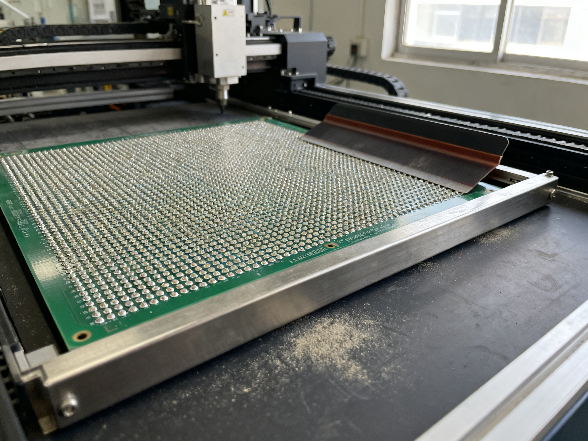
This article is about the 2026 reality of solder voiding: where voids come from, how you find the ones that matter, how you write acceptance criteria that survive a customer audit, and whether vacuum reflow actually earns its place on your line or is just an expensive way to solve a flux problem you haven’t diagnosed yet.
By the numbers
| Metric | Typical range on a high-density lead-free line | Why it matters |
|—|—|—|
| As-built void area inside a BGA ball, well-controlled line | Under 10% | Common customer drawing ceiling, with limits often set per-ball or per-location |
| As-built void area, struggling line | 20% to 30%+ | Usually a flux, soak, or stencil issue, not a component problem |
| Void inside a QFN thermal pad | Often 25% to 40% | Cosmetic to the eye, thermally and mechanically significant in high-power parts |
| Cost of a void-related field escape | Return freight, RMA investigation, line rework, scrap, and sometimes a full recall | Far more than the board that failed |
| Vacuum reflow cycle-time impact | Typically 10% to 30% longer than a conventional profile | The price you pay for lower void numbers |
Look, I’m not going to pretend there is a single industry-wide defect-rate chart for solder voiding in 2026. There isn’t a public, audited number that says “X% of boards ship with a void.” What exists is a much messier reality: internal quality data, customer-specific specifications, and a set of published standards that tell you what to measure but rarely tell you the one number that matters for your product. Be skeptical of anyone who gives you a clean industry-wide statistic.
What does exist are published specifications. IPC-A-610 and IPC-7095 both address voiding and porosity in BGA and bottom-terminated component construction, and the numeric limits you’ll see in practice (10%, 20%, 25%, or location-based rules) come almost entirely from customer drawings and customer-specific requirements, not from the standard itself. IATF 16949 and PPAP govern how you prove your process is capable and how you document changes. AEC-Q200, AS9100, MIL-STD-883, and ECSS-Q-ST-70-08 add qualification and documentation expectations for automotive, aerospace, and defence work. None of them hand you a magic void limit.
So why now, in 2026? Three things are pushing voiding risk up at the same time.
First, packaging density. Fine-pitch BGA, QFN with exposed thermal pads, LGA, and stacked-die parts leave less solder, thinner escape paths, and smaller gaps for gas to leave through. A ball that was “probably fine” in 2010 is a lot harder to fill cleanly today.
Second, lead-free chemistry. SAC305 and friends run at a melting point around 217°C, well above the 183°C of the old SnPb eutectic, and the alloys are less tolerant of oxidation and of poor wetting. Add in EU RoHS and REACH-driven restrictions, halide-free and low-halide flux requirements, and tighter water-soluble cleaning specs, and you have a process with less margin for a sloppy profile.
Third, paperwork. Automotive PPAP and defence qualification reviews get sharper every year. A customer who finds out about your voiding capability from a field failure, rather than from a process qualification package, will write requirements into your drawing that are much harder to meet.
Expert Tip: A void that looks scary in a fillet is usually a cosmetic trapped-gas bubble. A void inside a BGA ball or under a QFN thermal pad is where the risk actually lives. The dangerous ones are also the ones AOI cannot see, which is exactly why so many void escapes reach the customer. If you want the practical distinction between “looks bad on the microscope” and “fails in service,” plus guidance on when to stop trusting AOI and move to X-ray, that’s covered in the inspection section below.
One more thing worth saying up front, because it saves people months of wasted effort. Solder voiding is not a solder paste problem by default. It’s a gas problem. Something is generating vapour during reflow, and something is blocking its escape path. Understanding that sequence is what separates a fix that holds for three months from a fix that holds for three years.
This article is written by a process engineer at S&M Co. Ltd. (Shenzhen Chuxin Electronic Equipment Co., Ltd.), working with lead-free reflow and wave soldering lines for consumer electronics, semiconductor, and military electronics customers. A full author biography and reviewer credentials are published at the end of the article.
Ready to talk about your own void numbers? Bring us your current profile data or a set of X-ray images. We’ll help you work out whether the problem sits in the flux, the soak, the stencil, or the atmosphere, and whether a vacuum reflow upgrade would actually move your numbers. Talk to the S&M process engineering team.## About the Author
This article was written by a process engineer at S&M Co. Ltd. (Shenzhen Chuxin Electronic Equipment Co., Ltd.), where the author supports lead-free SMT reflow, wave soldering, and full line qualification for consumer electronics, semiconductor, automotive, and defence customers. Day-to-day work covers reflow profile development and troubleshooting on high-density BGA and QFN assemblies, with a focus on solder void root cause work.
[AUTHOR NAME — TO BE SUPPLIED]
Role: Process Engineer, SMT Reflow and Wave Soldering | S&M Co. Ltd.
Focus: Solder void root cause analysis, BGA and QFN reflow profiles, void acceptance criteria documentation, vacuum reflow qualification
Industries served: Consumer electronics, semiconductor, automotive, military, aerospace
Experience: [X YEARS — TO BE SUPPLIED] in SMT process engineering
Headshot: [AUTHOR PHOTOGRAPH TO BE SUPPLIED]
Credentials: [IPC-A-610 CERTIFIED SPECIALIST — TO BE SUPPLIED] | [IPC J-STD-001 SPECIALIST — TO BE SUPPLIED]
Author profile: [LINK TO AUTHOR PAGE — TO BE SUPPLIED]
Article reviewed and revised: 16 November 2026, by the S&M Co. Ltd. process engineering lead / customer quality manager ([reviewer credentials — IPC-A-610 Certified Specialist, 15+ years in SMT process engineering for defence and aerospace electronics]).
All bracketed fields must be completed from the author’s actual biography and credentials before publication.## Reading Voids Back to Their Causes: A Symptom-to-Cause Map
Diagnostics work far better when you start from the symptom rather than the void. The same pocket of gas can come from half a dozen different root causes, and the fix that helps one of them does nothing for the rest. Below is the map we actually use on the floor.
| Symptom you observe | Most likely cause | First check | What usually fixes it |
|—|—|—|—|
| Voids clustered along one edge or one corner of a BGA array | Blocked or restricted escape path, often a paste-print or stencil aperture problem | Compare stencil aperture coverage against the pad layout and the printed deposit thickness | Stencil aperture redesign, thinner deposit, longer soak before wetting |
| Voids concentrated in the thermal pad of a QFN or LGA | Gas outgassing from laminate, coating, or the exposed pad itself | Inspect the PCB stack-up and any conformal or solder-mask coating | Lower peak temperature, more aggressive ramp, pre-dry the board and the paste |
| Single large void in the middle of a ball | Trapped air from an unstable or over-thick deposit | Check paste slump and the printing deposit profile | Reduce deposit thickness, improve release, or re-bake the paste |
| Voids that appear only at the solder-to-pad interface | Poor wetting, oxidised or contaminated pad | Check pad surface condition and the cleanliness of the paste and no-clean flux | Improve pad cleaning, verify the pad finish, check paste age and storage |
| Voids that track with humidity or with storage time | Moisture in the laminate, prepreg, or paste | Log paste and board dwell time; compare wet and dry samples | Pre-dry components, control moisture, shorten the time between print and reflow |
| Random voids, no pattern, on multiple boards | Profile-driven, typically too short a soak or too steep a ramp | Pull the profile trace and confirm the actual board temperature | Adjust ramp, soak, and liquidus time; consider a vacuum-assisted reflow step |
| Voids that only appear in the first article, then improve | Cold or unconditioned component or paste | Check the reflow oven’s exhaust and temperature uniformity | Condition the oven, stabilise the line, verify thermocouple placement |
The three-question triage
When a customer sends a board back with a void complaint, three questions narrow the field quickly.
Where is the void relative to the joint? A void at the centre of a BGA ball points at gas generation and escape. A void at the interface points at wetting. A void in a corner of a large pad usually points at the stencil or at coplanarity. Location is the single cheapest diagnostic you have, and it is free because you already have the X-ray image.
Does the void pattern repeat? A repeatable pattern is a process or design problem: stencil, profile, pad finish, or laminate. A scattered, one-off pattern is usually material or handling: a wet board, an old paste jar, a cold part. If you can overlay several boards and see the same voids in the same places, stop changing the recipe and go look at the design.
Does the void area actually matter? IPC-A-610 treats solder voiding as a workmanship condition on non-hermetic joints, with acceptance generally tied to the proportion and location of voids rather than a hard count. Thermal and high-reliability programs usually write their own criteria, and those criteria, not the generic standard, are the ones that will be audited. Make sure your customer specification states a numeric void percentage, the measurement method (2D X-ray versus laminography versus cross-section), and the threshold location rules.
Why voids often survive the reflow oven and fail in the field
A void percentage measured on a golden board after reflow is a snapshot of one thermal cycle. Field failure comes from thousands. The two most common field complaints tied to voiding are thermal-pad overheating on a power device and intermetallic fatigue cracking in a BGA ball under repeated temperature cycling.
For the thermal case, the physics is straightforward: the exposed pad is the only path for heat to leave the die. Replace part of the solder with air and the thermal resistance of that pad goes up sharply, junction temperature rises, and the derating curve you designed against no longer applies. This is why a void under a thermal pad is often a higher-priority finding than a larger void in a signal ball.
For the fatigue case, the mechanism is a stress concentrator. Under temperature cycling, the CTE mismatch between the board and the package pushes and pulls on the solder, and the void boundary acts as a notch. Cracking usually initiates at the void edge or at the solder-to-pad interface and then propagates through the intermetallic layer. Add board flex, vibration, and moisture, and the joint has very little margin left.
Expert Tip: Void count is a poor proxy for risk; void location and void area fraction in the load path are the real metrics. If you are writing a specification or an internal process limit, define both the numeric threshold and the measurement method in the same sentence. An audit finding is almost always about the missing measurement method, not the missing limit.
Where a vacuum reflow step genuinely earns its cost
Vacuum-assisted reflow is not a cure-all, and it is worth saying so plainly. It reduces voids in the situations where the gas is already in the joint and only lacks a way out. That means voids trapped in a BGA ball, voids from an unstable or thick paste deposit, and voids caused by moisture release during the ramp. It does very little for a void caused by a contaminated or oxidised pad, and nothing at all for a void caused by a stencil defect, a coplanarity gap, or a missing escape path at the board surface.
If you are considering an upgrade, look at your own data first. Sort your X-ray findings by cause, not by appearance. If a meaningful share of your voids are gas-escape related, vacuum reflow has a strong case. If most of them are wetting and stencil issues, the money is better spent on print control, pad preparation, and profile work.
Next we walk through the measurement side: how to get a reliable void percentage, where 2D X-ray stops being enough, and how to write an internal limit that an auditor will accept.
Ready to talk about your own void numbers? Bring us your current profile data or a set of X-ray images. We will help you work out whether the problem sits in the flux, the soak, the stencil, or the atmosphere, and whether a vacuum reflow upgrade would actually move your numbers. Talk to the S&M process engineering team.## Root Causes of Solder Voiding: A Symptom-to-Cause Map
Strip away the jargon and solder voiding is one sentence: gas was generated, and gas had nowhere to go. Every root cause lives inside that sentence, so the useful way to organise causes is by where the gas came from and what stopped it from leaving.
The four cause families
| Cause family | Where the gas comes from | When it forms | Why it gets trapped |
|—|—|—|—|
| Material outgassing | Moisture in components, PCB prepreg, cleaning-water residues, conformal coating, low-Tg or halogenated flux residues | Mostly during ramp and soak, then again near liquidus | Flux devolatilises and the surface skins over before the gas has cleared |
| Flux exhaustion | Over-aged paste, wrong flux class for the alloy, too little flux deposited | Peak temperature, when the flux should still be active | No flux left to sweep the gas out of the molten pool |
| Thermal profile errors | Inadequate soak, steep ramp, low peak, time above liquidus too long, poor board-level uniformity | Anywhere in the profile | Gas evolves faster than it can migrate to a free surface |
| Geometry and design | Excess paste volume, small pad-to-window ratio on QFN, via-in-pad thermal patterns, warpage | Peak | There is no open path to the top of the joint |
That last row is the one people skip. A QFN thermal pad under a solder mask dam with no escape window can hold a void no process change will remove. A via-in-pad structure can wick solder downward and pull the pocket closed. You can profile around a geometry problem, but you cannot profile it away.
Fishbone view of the same thing
Solder voiding
├── Material
│   ├── Moisture in components (MSL handling)
│   ├── Prepreg and laminate outgassing
│   ├── Cleaning water residue
│   └── Conformal coating / solder mask
├── Flux
│   ├── Over-aged or open jar
│   ├── Wrong activity class for SAC305
│   ├── Too little flux volume
│   └── Contamination from paste handling
├── Thermal
│   ├── Short or cold soak
│   ├── Ramp too steep
│   ├── Peak too low
│   └── Time above liquidus too long
└── Geometry
    ├── Excess paste deposit
    ├── No escape window on QFN
    ├── Via-in-pad wicking
    └── Component or board warpage
Morphology tells you which family you are in
| Void morphology | Likely root cause | Verification method |
|—|—|—|
| Fine scattered porosity, most of the ball | Flux exhaustion or moisture outgassing | Paste age log plus a dry versus wet board comparison |
| One or two large round voids near the top of a ball | Gas trapped under a skinning surface, often a soak or ramp issue | Pull the profile trace, compare to board thermocouple |
| Void hugging the solder-to-pad interface | Wetting failure from oxidation or contamination | Cross-section and pad surface inspection |
| Void pinned to one corner of a pad | Print or stencil aperture defect, plus local geometry | SPI deposit map against stencil data |
| Void directly over a via | Via-in-pad or via wicking | Stack-up review and 2D X-ray overlay |
One customer line we worked with last year ran 20% to 30% voids inside its BGA balls and assumed a bad component lot. The paste log told a different story. The jar had been opened and left in a humid side room for weeks, and the soak was running cold and short, so the flux was spent before it could do any work. Fixing the paste handling and adding 30 seconds of soak dropped the same line to under 8% without touching the oven. On a different SAC305 line we chased a nitrogen atmosphere problem for weeks, and the actual fault was the nitrogen flow meter set far too high, which dried the joint surface before the flux could wet it. More atmosphere, more voids, opposite of the assumption.
Lead-free amplifiers
SAC305 and other silver-bearing SAC alloys melt around 217°C, well above the old 183°C SnPb eutectic. Longer dwell, higher thermal mass, thinner solder mask dams over exposed pads, and the loss of the anti-bubble aids found in some low-melt alloys all shrink your margin. Add halide-free flux requirements and you have less chemical buffer between a slightly wrong profile and a visible void.
That is why low voiding solder paste and better wetting matter so much in 2026. Lead-free solders tolerate bad wetting far less than tin-lead did.
Profile targets worth knowing by heart
| Stage | Lead-free SAC305 rule of thumb | Symptom of mis-set |
|—|—|—|
| Soak | 150°C to 180°C for 60 to 120 seconds | Cold or short soak brings scattered microvoids |
| Ramp | Controlled, roughly 1°C to 2.5°C per second | Steep ramp skips the drying window |
| Peak | 235°C to 245°C for the component | Low peak leaves poor wetting and slumping |
| Time above liquidus | 45 to 90 seconds | Too long burns off flux activity |
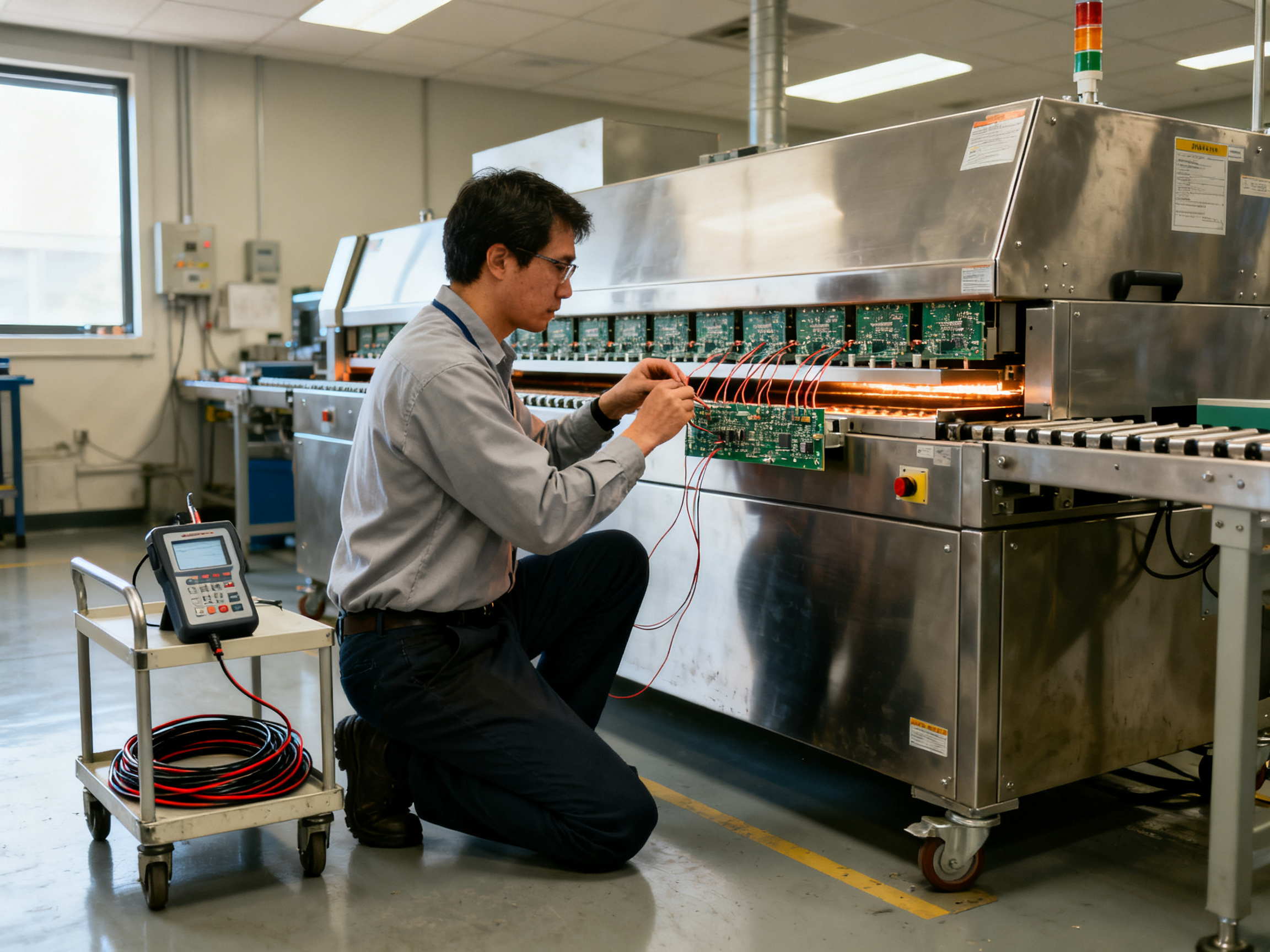
These are starting points, not gospel. Always confirm against your own board’s thermal mass and the datasheet of the part with the lowest profile rating.
Ready to talk about your own void numbers? Bring us your current profile data or a set of X-ray images. We will help you work out whether the problem sits in the flux, the soak, the stencil, or the atmosphere, and whether a vacuum reflow upgrade would actually move your numbers. Talk to the S&M process engineering team.## Inspection and Solder Void Analysis: Methods, Limits, and Void Calculation
Every void conversation eventually comes down to one question: how big is it, and where is it? The answer depends entirely on which tool you used to look. And the gap between what each method sees is where a lot of escapes begin.
What each inspection method actually sees
| Method | Detects | Misses | Destructive | Typical use |
|—|—|—|—|—|
| Visual / microscope | Fillets, exposed pad, missing solder on bottom-terminated parts | Every internal void | No | Incoming and rework check |
| AOI (2D optical) | Insufficient solder, missing components, exposed pad, some surface bridging | All buried voids inside a BGA ball | No | 100% inline screen |
| 3D AOI / AXI (inline X-ray) | Buried voids in larger balls, some pad voiding | Small voids, voids in fine pitch, geometry distortion | No | 100% inline on high-mix lines |
| 2D X-ray radiography (offline lab) | Void area and position in a defined region | Overlapping features, no depth | No | Sample-based failure analysis |
| Laminography / 2.5D | Depth-resolved voids in complex stacks | Very small voids below resolution limit | No | Advanced FA, high-reliability work |
| Micro-CT (3D) | True volume distribution, void shape | Cost, throughput, very small features | No | Root cause on design-level issues |
| Cross-section / metallography | Ground truth: voids, IMC thickness, cracks, wetting | Only the slice you cut | Yes | Failure confirmation, process qualification |
| SPI (solder paste inspection) | Deposit area, volume, offset, slump before reflow | Anything that happens in the oven | No | Root cause on print and paste issues |
AOI deserves a specific warning. It is an outstanding detector of missing solder and exposed pads on bottom-terminated components, which is exactly why it is trusted so much. It is blind to a void inside a ball, because the ball is closed. If a void matters to you, it will almost always be a void you cannot see optically.
X-ray has its own limits. At high magnification, geometric distortion shows up as void positions shifting from where they really are, which can quietly corrupt a positional acceptance rule. Small-diameter balls also sit near the resolution floor of a 2D system, so a 40 µm void in a 75 µm ball may be visible in one image and invisible in the next. What a datasheet calls resolution is a pixel size, not a guarantee of detectability. Treat it as a screening limit, not a promise.
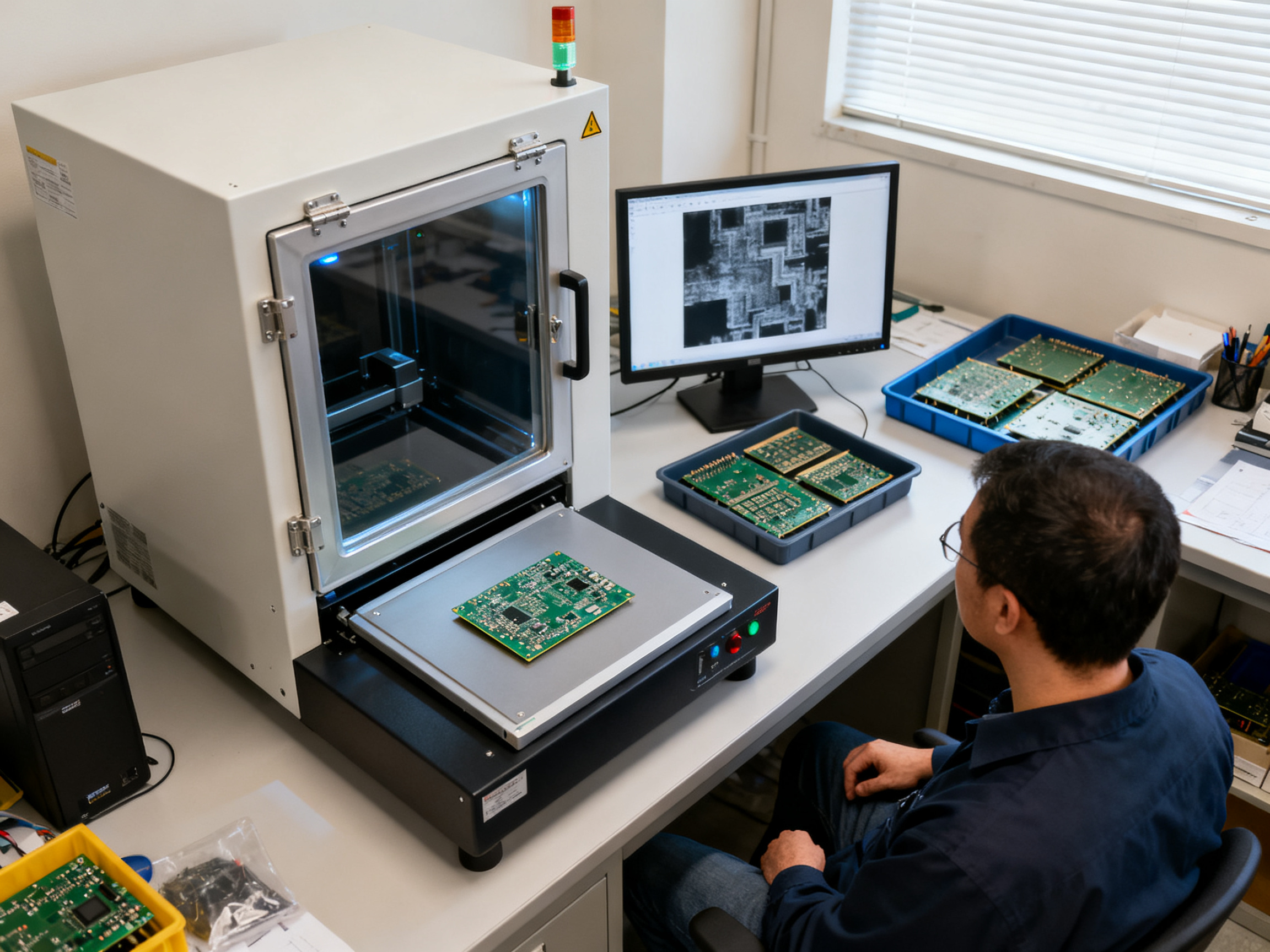
How solder void calculation works on the shop floor
The formula itself is short. Void percentage equals the total void area inside the defined region, divided by the total solder joint area in that region, multiplied by 100.
The hard part is the region. Three choices give three different answers on the same joint:
- Whole ball. Most common for BGA. A 30 µm void in a 400 µm ball is about 6% by this method.
- Solder fillet only. Sometimes used for part-level workmanship checks on QFN side joints.
- Thermal pad area. Standard for exposed-pad parts, where the void sits in a wide, thin deposit.
Two more decisions change the number. Sum all voids in the region, or measure only the largest single void? And are you measuring 2D projected area from an X-ray, or true 3D volume from CT? The wording in your specification has to settle all of it, because two qualified labs can produce legitimately different percentages from the same board.
Here is a worked example. A BGA ball measures 500 µm in diameter, giving a projected joint area of about 196,350 µm². The X-ray shows three voids measuring 8,000, 5,000, and 3,000 µm². Summed void area is 16,000 µm². Void percentage is 16,000 divided by 196,350, which comes out to 8.1%. Against a 10% limit, that joint passes. Against a customer rule that treats any single void over 5,000 µm² as a reject, the 8,000 µm² void fails on its own. Same image, two answers, one specification gap.
Pro Insight: When you write a void acceptance criterion, state four things in the same sentence: the numeric threshold, the region boundary, the measurement method, and the imaging resolution used. Add the segmentation threshold if you expect automated analysis. An audit finding is almost never about the missing percentage; it is about the missing method wording.
Writing criteria that survive an audit
IPC-A-610 is the workmanship acceptability reference for general soldering work, IPC-7095 covers BGA design and process guidance, and IPC-7525 covers stencil and solder paste printing. What none of them do is hand you the number for your product. In practice, void limits of 10%, 20%, or 25% come from customer drawings and customer-specific requirements, layered onto the workmanship standard. So separate the two layers in your documentation, and make sure your customer specification states the numeric limit, the region, and the method.
High-risk locations deserve their own rule, not a general percentage. Voids at the die edge, corner voids in a large deposit, and voids inside a thermal pad under a high-power device are usually treated as separate acceptance categories because that is where the mechanical and thermal consequence lives.
Sampling matters too. For ongoing control, most lines use X-ray on first articles plus a periodic sample. For failure analysis, cross-sectioning remains the only way to confirm intermetallic formation, cracking, or a wetting failure at the interface.
And a practical note on where this sits in the line: your reflow profile data and your X-ray void maps belong on the same dashboard. S&M Co. Ltd.’s reflow and wave soldering lines feed the same process data into inline inspection and sample-based analysis, so a profile change and its void response can be compared on the same board rather than argued about from memory.
Ready to talk about your own void numbers? Bring us your current profile data or a set of X-ray images. We will help you work out whether the problem sits in the flux, the soak, the stencil, or the atmosphere, and whether a vacuum reflow upgrade would actually move your numbers. Talk to the S&M process engineering team.## Vacuum Reflow vs. Conventional Reflow: How Each Machine Removes a Void
From the loading end, a vacuum reflow oven and a conventional one look like the same machine. Same conveyor, same nozzle, same zone count. The difference shows up in the last 30 seconds of the profile, and it explains most of the void reduction you see in the X-ray data.
In a conventional oven, the only place trapped gas can go is back out through the solder joint it came from. That is a narrow, sometimes non-existent path. A QFN thermal pad is the classic case: a wide, thin deposit sitting on a board surface with almost no open volume above it, so the gas has nowhere to travel and simply stays.
Vacuum reflow changes the physics rather than the chemistry. The chamber is evacuated after the solder has melted and the joint has already collapsed. The resulting pressure differential pulls the molten solder inward and shrinks the joint volume, forcing the trapped gas toward the joint’s vent path and out. The void does not get “removed” so much as compressed and expelled while the solder is still fluid.
Conventional reflow
   Gas trapped inside joint -> only exit is back through the joint -> void stays

Vacuum reflow
   Joint collapses under pressure differential
   Gas is driven toward the vent path
   Void volume shrinks or clears
Side-by-side comparison
| Factor | Conventional reflow | Vacuum reflow |
|—|—|—|
| Void removal mechanism | Gas escapes through the joint as it forms | Pressure differential collapses the joint and drives gas to the vent path |
| Typical BGA ball void result | Baseline, often 5% to 20% depending on process | Often 2% to 8% on gas-escape-limited joints |
| QFN thermal pad result | Often 25% to 40% void on wide deposits | Large drops, but only where an escape path exists |
| Wetting and intermetallics | Determined by paste, flux, and profile | Same wetting behaviour; vacuum can improve wetting by pulling molten solder into the pad |
| Cycle time | Baseline | Typically 10% to 30% longer, plus evacuation and recovery time |
| Energy use | Lower | Higher, from the vacuum pump and faster ramp compensation |
| Board format limit | Wide range | Chamber size caps panel and board dimensions |
| Risk points | Low | Solder splatter, profile distortion if vacuum is too aggressive, pump maintenance |
| Cost class | Standard capital | Premium capital, plus consumables and service |
From Our Experience: On customer lines running vacuum-assisted reflow in 2026, BGA ball void averages moved from roughly 12% to 18% down into the 3% to 6% range, and QFN thermal pad voiding dropped from the high 20s into single digits. The pattern we see most often is that a void caused by a wetting problem, a stencil defect, or a coplanarity gap does not improve at all. Vacuum fixes gas that is already inside a good joint and has nowhere to go. It does not fix a joint that never wetted in the first place. Cycle time on those lines ran 15% to 25% longer, and the vacuum level had to be tuned per board family; too aggressive and we saw solder splatter on the escape vents.
The capital decision
Think of it in terms of payback, not price. If a line is scrapping or reworking a thousand boards a year at 40 to 60 dollars of rework cost per board, the arithmetic moves fast. If the void problem is 0.5% of volume and the joint is a 0402 signal pad, a vacuum oven will never pay back, and the money belongs in print control and profile work instead.
Vacuum reflow earns its place on defence, aerospace, and automotive lines, on high-mix BGA programmes with tight thermal-pad limits, and on any line where the customer drawing specifies a hard void percentage inside the ball. On commodity consumer electronics with mature stencil and paste control, conventional reflow plus X-ray sampling usually gets you to the same acceptance limit for a fraction of the capital.
Ready to talk about your own void numbers? Bring us your current profile data or a set of X-ray images. We will help you work out whether the problem sits in the flux, the soak, the stencil, or the atmosphere, and whether a vacuum reflow upgrade would actually move your numbers. Talk to the S&M process engineering team.## PCB Void Reduction: The Process Toolkit That Actually Works
Most void problems get fixed in the wrong order. Somebody opens a new jar of paste, watches the numbers move a bit, then buys a vacuum oven, and the void count improves right up until the jar runs out. That is backwards. Process first, material second, capital last.
Here is the toolkit we reach for, roughly in the order it pays back.
1. Get the profile right before you buy anything
Most “void problems” we are sent to look at are profile problems wearing a costume. Soak controls two things at once: it drives moisture out of the laminate and components, and it activates the flux so it has something to say when the solder melts.
The rule of thumb for SAC305, which is where most of the industry sits in 2026:
| Stage | Target | What breaks when you miss it |
|—|—|—|
| Soak | 150°C to 180°C for 60 to 120 seconds | Scattered microvoids, flux that arrives at liquidus already tired |
| Ramp | 1°C to 2.5°C per second | Steep ramp skips the drying window entirely |
| Peak | 235°C to 245°C at the component | Low peak means poor wetting and slumping |
| Time above liquidus | 45 to 90 seconds | Too long burns off flux activity, too little means incomplete collapse |
Now the part most people skip. Profile the board, not the oven. Put at least three thermocouples on a representative board: one on a small component, one on a large thermal mass, one near a BGA array. A profile that looks beautiful on a coupon board can be 25°C colder on the part that actually matters, and you will spend a week blaming the paste.
Nitrogen atmosphere helps where oxidation is the driver, mostly on fine-pitch and long dwell profiles. It is not a void fix by itself, and running too much flow dries the joint surface before the flux can wet it. We have chased exactly that mistake on a SAC305 line and found the flow meter set far too high.
Expert Tip: The three settings that account for most of the void improvement we see in production lines are soak time, peak temperature, and paste deposit volume. Everything else is fine tuning. If you only get to change one thing, add 30 seconds of soak and re-run the X-ray before you touch a single other variable.
2. Print-side fixes, which are usually free
A void in a wide deposit is often a geometry problem wearing a process costume.
- Reduce deposit volume on thermal pads. A QFN pad that gets too much paste has no room to collapse. Trim the aperture or step the stencil down.
- Balance aperture count. Uneven aperture distribution across a BGA array prints uneven thickness, and thin spots collapse better than thick ones, so voids land on the thick side.
- Fix the solder mask dam. An undersized dam or a misregistered dam closes the escape path at the board surface. This is the one void cause no amount of vacuum will touch.
- Plan for via-in-pad. Wicking solder down a via pulls the pocket closed. Full or tent the via, or accept that the design owns that void.
Expert Tip: If you see voids sitting right over a via in every board, stop blaming the paste. Via-in-pad wicking is a stack-up decision, and it needs a design change or a via-fill process, not a better recipe.
3. Material handling and component-side fixes
This is where a surprising amount of voiding hides.
Low voiding solder paste is a real lever in 2026. Modern formulations use a low-residue, high-activation flux with controlled outgassing, so you get flux action without the gas that creates the void in the first place. When you switch to a low voiding paste, retune the profile. These pastes often have a narrower process window than a general-purpose paste, and dragging a profile built for one formula onto another is a classic way to make things worse.
Moisture control follows the MSL rules in J-STD-033, and handling in the field follows J-STD-020. Bake components that come out of dry cabinets with a known exposure, and pre-dry the boards themselves if the laminate is the suspect. A vacuum oven used as a drying oven is a mistake we still see; the gas you are trying to remove needs somewhere to go.
Watch the board stack-up too. Low-Tg laminates and high moisture uptake prepregs outgas at temperatures that are harmless for a standard mid-Tg FR-4. Ask your laminate supplier for their outgassing and moisture absorption figures, and if they do not have them, that is a supplier qualification problem, not a solder problem.
4. Design and prevention for the next programme
The cheapest void is the one you designed out.
| Lever | Effect | Cost | Lead time | Best for |
|—|—|—|—|—|
| Profile optimisation (soak, peak, TAL) | Large | Free | Days | Almost every line |
| Paste volume and aperture reduction | Medium to large | Low | Weeks | QFN thermal pads, large deposits |
| Stencil step-down and aperture balancing | Medium | Low | Weeks | BGA arrays, uneven deposits |
| Solder mask dam and aperture redesign | Large | Low | One PCB spin | Closed escape paths |
| Low voiding solder paste | Medium | Low to medium | Weeks | Wide deposits, high void sensitivity |
| Baking and moisture control | Medium | Low | Days | Humid regions, long storage |
| Nitrogen atmosphere | Small to medium | Medium | Months | Fine pitch, long dwell |
| Via fill or tenting | Large | Medium | One PCB spin | Via-in-pad structures |
| Vacuum reflow | Large on gas-escape voids | High | Months | High-reliability, hard limits |
| Pad geometry and thermal via array (DFM) | Large | Free at design stage | One programme | New designs |
That last row is the one nobody budgets for and everybody should. Publish DFM rules to your customers: pad-to-window ratios, thermal via arrays under exposed pads, keep-out zones around large thermal areas, and a recommended paste volume per pad. Then put a void limit on the drawing that you can actually measure.
A quick routing guide
Void found on X-ray
│
├─ Void hugging solder-to-pad interface?
│   └─ Wetting problem → check pad finish, paste age, cleaning, contamination
│
├─ Void over a via?
│   └─ Via-in-pad wicking → fill, tent, or redesign
│
├─ Void in a corner of a wide pad?
│   └─ Print or stencil → reduce deposit, rebalance apertures, check release
│
├─ Void clustered along one array edge?
│   └─ Restricted escape path → check mask dam, stencil coverage, deposit thickness
│
├─ Random voids, no pattern?
│   └─ Profile or material → soak time, peak, paste condition, moisture
│
└─ Void is thermal-pad wide and large?
    └─ Gas trapped under a skinning surface → longer soak, vacuum reflow, low voiding paste
From Our Experience: The cheapest void improvement we have measured came from a customer who changed nothing but the paste handling and added 30 seconds of soak, taking a 20% to 30% BGA line to under 8%. The most expensive project we have worked on was a vacuum oven installed on a line whose real problem was a closed solder mask dam. Both teams thought they were buying the answer. Only one of them was right.
Ready to talk about your own void numbers? Bring us your current profile data or a set of X-ray images. We will help you work out whether the problem sits in the flux, the soak, the stencil, or the atmosphere, and whether a vacuum reflow upgrade would actually move your numbers. Talk to the S&M process engineering team.
Low-Void Paste, Flux Selection, and What “Void-Free Soldering” Actually Means
Let’s kill a myth first. There is no void-free soldering process. Nobody has ever run a line where X-ray came back clean on every ball, every cycle, forever. What the industry actually sells and qualifies against is void reduction to a controlled target, expressed as a maximum void percentage per device type and per location, verified by X-ray sampling against a written acceptance criteria.
So when a paste vendor says “low voiding”, read it as “narrower distribution and a lower average”, not “zero”. The useful question is what number moves, and at what cost to your process window.
Choosing a paste on measurable criteria, not on the label
| Flux family | Activity | Halide spec | Outgassing behaviour | Typical void result |
|—|—|—|—|—|
| No-clean, general purpose (ROL0-style chemistry) | Low to medium | J-STD-004 limits, often below 0.05% by weight | Moderate, solvent content dominates early ramp | Baseline 5% to 20% in BGA balls, heavily profile dependent |
| No-clean, low voiding formulation | Medium, tuned activation | J-STD-004 compliant, low ionic residue | Controlled, flux burns off cleanly near liquidus | Often 2% to 8% in gas-escape-limited joints |
| High activity no-clean | High | Halide content higher, residue and corrosion risk rise | Aggressive early, risk of premature burnout | Lower voids in some setups, but skinning and residue risk |
| Water-soluble | High | Halide free | Heavy outgassing if the profile is not matched | Low voids, plus strict cleaning and cleanliness spec cost |
Halide limits and residue testing come from J-STD-004, and moisture handling from J-STD-020 and J-STD-033. Match the flux to the alloy, the component termination, and your cleaning regime. A no-clean line cannot suddenly adopt a water-soluble paste without bringing in residue testing and a new cleaning scope.
Also check the shelf life and bake life, then log it. An open jar of paste in a humid room is the same root cause as a cold soak, wearing a different hat.
Why the most active flux is not the best void-free flux
Over-activity buys you flux action you may not need and residue, corrosion risk, or premature solder mask degradation you definitely do not. And switching to a low voiding paste usually means retuning the profile, because these formulations often carry a narrower process window than a general-purpose paste.
And do not skip wetting
Poor wetting is one of the most common solder void root causes. A joint that wets well vents gas out through the joint. A joint that does not wet traps it. We unpack the wetting primer in the section that follows, because getting the flux and the wetting behaviour right together is where most of the void reduction actually comes from.
Ready to talk about your own void numbers? Bring us your current profile data or a set of X-ray images. We will help you work out whether the problem sits in the flux, the soak, the stencil, or the atmosphere, and whether a vacuum reflow upgrade would actually move your numbers. Talk to the S&M process engineering team.## Wetting Fundamentals: The Root Cause Hiding Behind Most Voids
Wetting in soldering means molten solder spreading across a solid surface. It happens when the solder’s surface energy is lower than the surface energy of the thing it is touching, so it flattens out and clings instead of beading up. Young’s equation describes the balance, and the number everybody watches is the contact angle, θ. Low angle means the solder spread wide and hugged the surface. High angle means it pulled back into a bead.
   Good wetting: θ < 30°        Poor wetting: θ > 90°
      _______                     ___
     /       \                   /   \
    |    ___  |                 |  ( )  |
    |___/   \__|                 \_____/
       \___/                      bead
Here is the link to voids that people miss. During reflow, the joint has to stay open along the solder mask and pad boundary long enough for volatile species to escape. Poor wetting closes that escape path early. The gas stays inside the joint and becomes a void. So wetting failure and solder voiding are usually one problem wearing two names.
Wetting is also something you can measure, which is nice.
| Surface finish | Typical contact angle | Void tendency |
|—|—|—|
| ENIG (immersion gold) | 15° to 35° | Low |
| HASL, fresh | 40° to 60° | Medium |
| OSP | 30° to 50° | Low to medium |
| Oxidised or contaminated pad | 90° and above | High |
Test it with a witness coupon: a coupon of the same surface finish, a defined volume of solder, and a spread test measuring the area covered. Contact angle measurement on a cross-section gives a cleaner number for work that needs documentation.
The acceptance target usually sits below 90°, with 30° or 45° preferred for higher reliability work. Your customer drawing is what actually governs.
One practical note. We have seen a QFN joint with textbook wetting that still trapped a large void, purely because the deposit was too thick to collapse. Wetting is the root cause hiding behind most voids, but it is not the only one. Pair it with the profile and geometry checks from the toolkit section.
Ready to talk about your own void numbers? Bring us your current profile data or a set of X-ray images. We will help you work out whether the problem sits in the flux, the soak, the stencil, or the atmosphere, and whether a vacuum reflow upgrade would actually move your numbers. Talk to the S&M process engineering team.## Implementing Void Reduction on a Production Line: A 90-Day Roadmap
Voids do not get fixed in an afternoon. They get fixed in phases, and the phases matter, because the wrong order is how lines end up with a shiny new vacuum oven and the same defect rate.
Here is the plan we hand customers who want a defensible, documented improvement rather than a lucky result.
Phase 1, weeks 1 to 3: establish the baseline
You cannot reduce what you have not measured, and you cannot defend a number you cannot reproduce.
- Write the criteria first. Put the numeric void limit, the region boundary, the measurement method, and the imaging resolution into the drawing or the wording note before you collect data. Otherwise you are measuring whatever your lab happens to report.
- Sample the current population. X-ray a representative set, not the good board you found in the finished goods rack. Twenty to thirty samples spread across lots, shifts, and ovens.
- Build a Pareto. Classify each void by device type and defect location, then rank them. Interface voids, gas voids, corner voids, thermal-pad voids. The top two categories usually own 80% of your risk.
- Confirm profile and moisture control. Pull the profile traces and check the paste and component bake logs. If these two are not under control, everything after this phase is guesswork.
Phase 2, weeks 4 to 8: run the cheap levers
Spend nothing on capital in this phase. Exhaust the free and low-cost fixes first.
- Re-tune the profile using multi-thermocouple profiling on a representative board, not a coupon.
- Run paste and paste-volume trials, including a low voiding solder paste comparison.
- Optimise stencil apertures, step-downs, and aperture balance.
- Tighten component bake and handling discipline per J-STD-020 and J-STD-033 practice.
- Then re-X-ray the same sample set and see what moved.
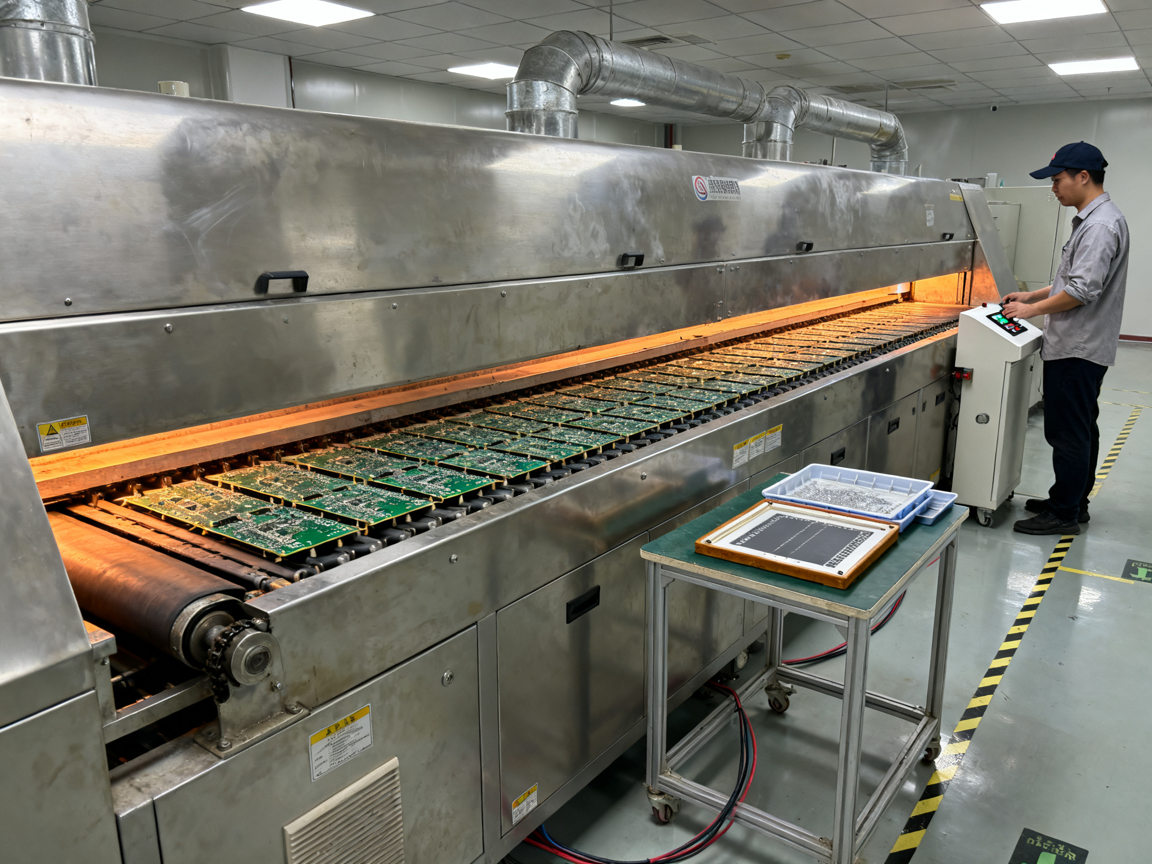
If the residual voids are still gas-escape limited after all that, you have a real capital case. If they are not, a vacuum oven will not help.
Phase 3, weeks 9 to 12: capital evaluation and qualification
- Pilot vacuum reflow on one line and one board family.
- Build a before and after X-ray dataset from the same population.
- Run a capability study (Cpk) against the agreed criterion, not against a number you picked last week.
- Update the control plan, train operators, and assemble the customer and audit documentation package.
Governance that keeps it from drifting
| Control plan parameter | Spec | Method | Frequency | Reaction plan |
|—|—|—|—|—|
| Soak time and temperature range | 150°C to 180°C, 60 to 120 s | Board-level thermocouple profile | Every lot | Stop, re-profile, hold material |
| Peak temperature at the part | 235°C to 245°C | Profile trace, board sensor | Every lot | Quarantine lot, check thermocouple placement |
| Time above liquidus | 45 to 90 s | Profile trace | Every lot | Adjust and re-run first article |
| Paste deposit volume | Per aperture spec | SPI | Every lot | Stop and rebalance stencil |
| Component bake and floor life | Per J-STD-033 handling | Bake log and MSL labels | Every receipt | Quarantine and re-bake |
| X-ray void sampling | Per drawing sampling plan | 2D X-ray or laminography | First article plus periodic | Escalate to failure analysis |
| Solder mask dam and via condition | Design specification | Incoming and X-ray review | Per lot | Escalate to design |
Escalation rules matter more than people think. Write down, before you need it, what happens when a sample fails: who gets called, how much material is held, and what the requalification path is. A line without a written reaction plan tends to negotiate instead of contain.
Training checklist for line operators and quality engineers: read the profile, place thermocouples correctly, log bake and paste times, interpret an SPI deposit map, recognise a void on a radiograph, and know when to stop the line.
And here is the ROI calculation people forget to do. Typical input ranges for a simple model are rework or scrap cost per board (typically $40 to $120), annual volume, current void-related reject rate (often 0.5% to 5%), and expected void reduction from the chosen fix. Multiply, compare to equipment cost plus training plus consumables, and set a payback window. If the model says 3 years, you have a business case to present, not a guess.
From Our Experience: The best 90-day results we have seen came from lines that did phase 1 properly and then stopped. One customer finished phase 2 at under 8% void on BGA balls, wrote the criteria into their drawing, and never bought a vacuum oven. Another skipped to phase 3, installed the oven, and spent three months explaining to their customer why a closed solder mask dam was still producing voids.
Ready to talk about your own void numbers? Bring us your current profile data or a set of X-ray images. We will help you work out whether the problem sits in the flux, the soak, the stencil, or the atmosphere, and whether a vacuum reflow upgrade would actually move your numbers. Talk to the S&M process engineering team.## Conclusion: The Author’s Expert Perspective and Next Steps
Here is the whole argument in one line: solder voiding is a process-control problem first and an equipment problem second. Most of the improvement you can get comes from profile, moisture control, flux and paste matching, and paste volume. Vacuum reflow is an accelerator, and it is the right accelerator for high-reliability, high-mix lines. It is a poor substitute for a diagnostic you never did.
Recap checklist: 10 questions to ask your SMT equipment supplier about void reduction
- Does the vacuum stage collapse the joint, or only hold the chamber below atmosphere?
- What chamber size, and what board formats fall outside it?
- What vacuum level do you recommend per board family, and what happens when it is too aggressive?
- How much cycle time does the vacuum stage add?
- Can you show before and after X-ray data from a line like mine?
- How is the profile re-tuned when vacuum comes on?
- What solder splatter containment do you provide?
- What pump maintenance interval and consumable cost per year?
- Can your line integrate with our inline X-ray or 3D AXI for closed-loop feedback?
- Will you support a paid trial with measured before and after data on my assemblies?
Ranked recommendations by buyer type
| Line type | Pull these first | Demand this specification language |
|—|—|—|
| Consumer electronics, high volume | Profile and soak, paste handling and bake, paste volume, stencil balance | Limit plus region plus method, sampled by X-ray on a stated frequency |
| Semiconductor and back-end packaging | Paste volume control, low voiding solder paste, inline AXI data as a process signal | Maximum void area fraction per ball, automated segmentation threshold stated |
| Military and aerospace | Everything above, then vacuum reflow, plus cross-section and laminography | Location-based rules for die-edge and thermal pad voids, resolution stated, Cpk demonstrated |
Three next steps. Request an X-ray baseline of your top three highest-risk assemblies, distributed across lots and shifts. Write the void acceptance criteria into the drawing or the wording note before you collect more data, stating the numeric limit, the region boundary, the measurement method, and the imaging resolution in the same sentence. Then schedule a vacuum reflow trial with measured before and after data on the same population, and only commit capital if the residual voids are still gas-escape limited.
Ready to talk about your own void numbers? Bring us your current profile data or a set of X-ray images. We will help you work out whether the problem sits in the flux, the soak, the stencil, or the atmosphere, and whether a vacuum reflow upgrade would actually move your numbers. Talk to the S&M process engineering team, or explore our lead-free reflow ovens, wave soldering machines, and complete SMT lines.