
Published: 24 October 2026
Reading Time: 21 minutes
Reviewer: [Reviewer Name, TBD]
Reviewer Credentials: [Reviewer credentials, TBD, e.g. SMT Process Engineer, IPC Certified Specialist, to be assigned before publication]
Two years ago, a customer in Dongguan sent us a controller board with a fault that had them pulling hair. Every board tested fine on the line. Every board failed in the field, and the failures clustered around one connector that was soldered by hand.
The fix was not a better iron. It was a better process decision. That board now runs through a selective welder with a programmed nozzle path, and the field returns stopped overnight.
That kind of story plays out in almost every factory we walk into. The board itself is rarely the problem. The soldering process was picked for the wrong reason, usually because the machine was already on the floor or because someone copied what the last customer did.
Why this decision is harder now than it was five years ago
Soldering used to be a fairly simple choice. If your board was surface mount, you reflowed it. If it had through-hole parts, you waved it. Things are not that clean in 2026.
Boards now pack BGA and QFN packages right next to big power connectors and heat-generating parts. Lead-free alloys run hotter and behave differently under thermal cycling than tin-lead ever did. Automotive, aerospace and defence customers want full traceability and documented process capability. And labour costs, energy prices and nitrogen supply all sit right on the same spreadsheet as your process engineer.
Nobody can optimise everything at once. That is the honest version of the wave soldering vs reflow question. So let’s break it down properly.
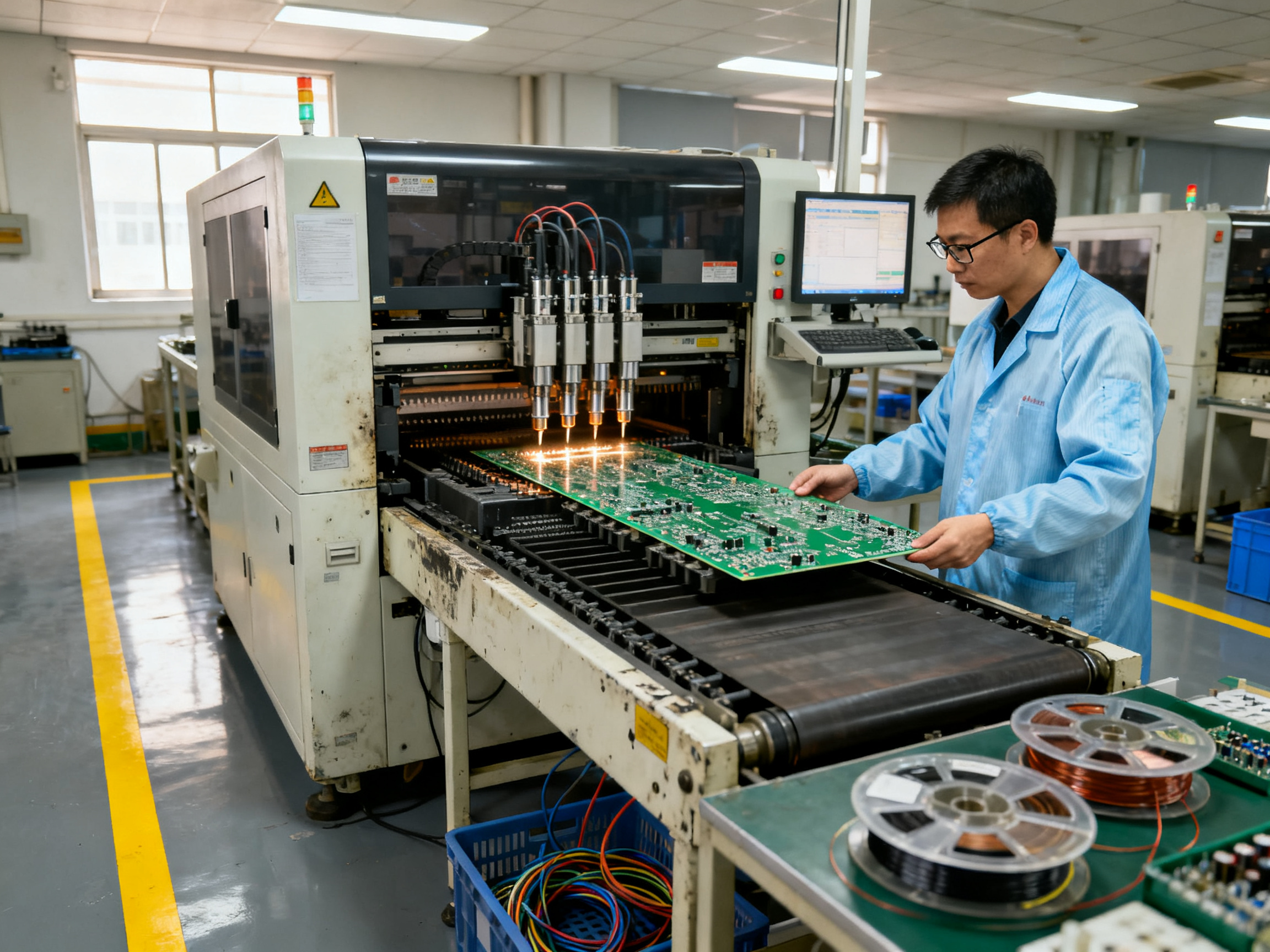
| Process | Best fit | Main strength | Main headache |
|—|—|—|—|
| Reflow (oven) | Dense SMT, BGA, QFN, fine-pitch | Thousands of paste-defined joints soldered in one controlled profile cycle | Hidden joints, voiding, warpage, profile control |
| Wave soldering | Many accessible through-hole joints on an open board | Very high simultaneous throughput | Broad thermal exposure, dross, masking, bridging |
| Selective soldering | A few through-hole joints surrounded by dense SMT | Solder applied only where you program it | Capital cost, programming, nozzle and fixture work |
| Hand soldering | Prototypes, repairs, one-off joints | Maximum flexibility, almost no setup | Operator variation, labour cost, traceability |
What the standards actually say
Here is where a lot of buying guides get vague. The industry standards do not hand you a decision chart. They hand you a set of constraints.
IPC J-STD-001, the main workmanship and process-control standard for soldered assemblies, covers materials, methods, acceptance criteria and process control across reflow, wave and hand methods. Its public table of contents confirms that framing, but the normative detail sits behind a licence, so treat vendor process windows as planning inputs rather than as standard limits. You can see what the document scope covers in the IPC J-STD-001 table of contents.
What is genuinely open and useful is NASA GSFC-STD-6001A, Guidelines for Temperature Profiling for Mass Soldering Processes. It covers profiling for both reflow and wave, and it references radiographic inspection of area-array joints. If you solder BGAs, that is the document worth reading end to end.
Moisture-sensitive components bring their own rulebook. The JEDEC and IPC J-STD-033 series covers handling, packing, shipping and use of moisture and reflow sensitive devices, which matters enormously when your parts sit for weeks between print and place and placement. And hand soldering is not a free-for-all either; NASA guidance covers soldering iron tip grounding checks and periodic verification, which is a small thing that catches people out during audits.
So the honest framing for 2026 is this: soldering process selection is a product and process-control decision, not a shopping decision.
The forces pushing the decision in 2026
Miniaturisation has changed the failure modes. Fine-pitch leads bridge when the wave of molten solder touches a broad area of the board underside. QFN exposed pads void when there is too much or too little solder under them. BGA joints hide opens from visual inspection entirely. A process that gives you clean, shiny, visible joints can still be producing a 20 percent void under a QFN pad.
Mixed assemblies force sequencing. Most real products need reflow for the SMT population, then a second step for through-hole parts. Whether that second step is wave, selective, pin-in-paste reflow, or a controlled hand operation depends on how open the board is and how close those pins sit to sensitive components.
Lead-free narrowed the thermal margin. SAC-type alloys generally need higher process temperatures than tin-lead. Stiffer joints, faster intermetallic growth, and more sensitivity to copper dissolution all show up in fatigue life. That is why design changes, bigger pads and sometimes underfill now appear in boards that never needed them before.
Energy and nitrogen are line items now. Oven zone count, conveyor speed, board thermal mass, pot temperature, preheat and nitrogen purity all affect your cost per conforming board. One 2026 market analysis notes that nitrogen atmosphere reflow is becoming standard in high-reliability production while also pushing operating costs up, which is worth reading alongside any equipment quote. See the 2026 soldering equipment market analysis for a sense of the trend.
High-mix lines changed the maths. If you run twelve board families with small batch sizes, the metric that matters is cost per conforming assembly, not cycles per hour. A wave machine that is brilliant on one open board can be a bottleneck on a shop with constant changeovers.
None of this is one source’s opinion. It is the pattern across process standards, qualification practice and what we see on installed lines every week.
How to read the rest of this guide
We will walk through the reflow soldering process and the wave soldering process mechanically, temperature by temperature, then get into the parts people argue about: defect rates, joint reliability, throughput, cost of ownership, and where selective soldering beats wave soldering and where plain hand soldering is still the right call.
The goal is not to tell you which machine to buy. It is to help you match your product, your volume and your quality requirements to a process you can actually qualify and document.
One more note on evidence. Much of what is published on this topic comes from equipment suppliers and market report firms, not from IPC or peer-reviewed research. We will say so when we use those numbers. Treat them as planning inputs, not as acceptance criteria, and always validate with your own thermal cycling, cross-sectioning and X-ray data.
[AUTHOR NAME, TO BE SUPPLIED]. As a [role and title] with S&M Co. Ltd. (Shenzhen Chuxin Electronic Equipment Co., Ltd.), an SMT equipment manufacturer specialising in lead-free reflow ovens, wave soldering machines and complete SMT production lines, [AUTHOR NAME] works directly with consumer electronics, semiconductor, automotive, military and aerospace manufacturers on soldering process selection, defect reduction and line integration for high-density assemblies. Hands-on work with BGA and QFN-heavy boards and lead-free conversion projects means the guidance below is grounded in installed-base realities, not theory. [AUTHOR NAME] holds [years of experience, installed line count, certifications such as IPC-A-610 Certified Specialist], to be verified before publication.
This article is reviewed by [Reviewer Name, TBD].