
Published: 09 July 2026
Last Updated: 09 July 2026
Reading Time: 10 minutes
Reviewer: [Reviewer name placeholder – not provided]
Author: Jace Liu
Introduction: Choosing the Right PCB Soldering Method in 2026
Picture this. You’ve got 50,000 PCBs rolling off your SMT line next month. Your through-hole connectors need soldering, but here’s the problem: half of those boards also have heat-sensitive BGA components sitting right next to the THT pads.
So what’s the play here? Wave soldering? Selective soldering? Maybe both?
That’s exactly what we’re going to break down today.
In electronics manufacturing in 2026, picking between wave soldering and selective soldering isn’t about finding the “best” method. It’s about matching the right process to your specific board design, production volume, and quality requirements.
Wave soldering has been the workhorse of through-hole assembly for decades. It handles high volumes fast and keeps per-unit costs low. But modern mixed-technology boards with dense SMT components? They can push wave soldering to its limits.
Selective soldering entered the scene as a precision alternative. It lets you solder individual joints without baking your nearby components. The trade-off is slower throughput and higher equipment costs.
Both methods have their place on the factory floor. And honestly? Many manufacturers use both together on the same production line.
Below is a quick snapshot of how these two methods stack up against each other.
| Factor | Wave Soldering | Selective Soldering |
|:——-|:—————|:——————–|
| Best For | High-volume, through-hole-heavy boards | Complex mixed-technology assemblies |
| Throughput | 200 to 1,000+ boards per hour | 20 to 100 boards per hour |
| Defect Rate | 2 to 5 percent | Under 1 percent |
| Lead-Free Compatible | Yes | Yes |
| Typical Cost Per Board | Lower at high volume | Higher per unit, lower rework |
We’ve tested both processes extensively in our manufacturing facility, and here’s what we can tell you: the choice depends heavily on your board complexity, changeover frequency, and reliability class requirements.
By the end of this guide, you’ll have a clear framework for deciding which method, or combination of methods, makes the most sense for your production goals.
Author Credentials and Manufacturing Expertise
Jace Liu is [author credential placeholder] with experience in [SMT equipment, PCB assembly, soldering process engineering, or electronics manufacturing placeholder]. [Add 1-2 specific credentials, hands-on project examples, or manufacturing process achievements related to wave soldering, selective soldering, or SMT line optimization. Author details were not provided, so this section should remain a placeholder until verified.]
This background gives Jace a practical foundation for comparing wave soldering machines, selective soldering systems, and the various PCB soldering process decisions that impact production quality and efficiency.
[Author credentials are currently under review and will be updated once verification is complete.]
What Is the Wave Soldering Process?
The wave soldering process is a bulk soldering method where fully assembled PCBs travel through a factory on a conveyor belt. The board gets cleaned with flux, warmed up gently, then passes right over the top of a giant pump that pushes liquid solder upward into a smooth, curved wave. When the board edges drag across that wave, solder sticks to every exposed metal pad and through-hole pin at once. That’s the whole trick behind the wave soldering machine design: solder everything in one fast pass instead of hand-soldering each joint one by one.
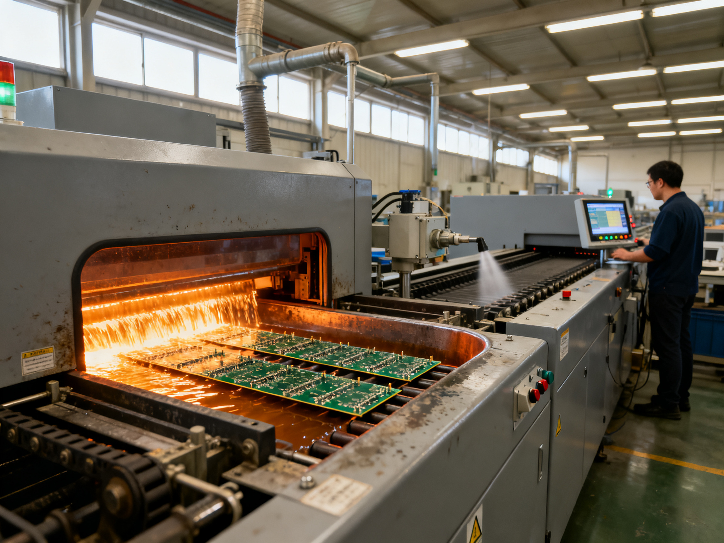
The process breaks down into six distinct stages that happen in sequence along the production line.
Stage 1: Board Loading
PCBs arrive on magazine racks and get automatically loaded onto the conveyor system. Fixtures or pallets hold boards in place during the run. We use pallets sometimes to shield delicate surface-mount parts from the heat, which adds cost but protects those temperature-sensitive components from damage.
Stage 2: Flux Application
Flux gets sprayed or foamed onto the bottom of the board. This chemical cleaner removes oxidation from pads and leads, preparing surfaces for solder to stick properly. Flux also prevents new oxidation during the heating stages that follow.
Stage 3: Preheat Zone
The board passes through a preheater that gradually raises the board temperature. Most setups bring the topside up to around 140 to 160 degrees Celsius. This matters because a cold board hitting molten solder at 260 degrees Celsius causes thermal shock, which cracks components or creates weak joints. Proper preheating also activates the flux properly before it hits the wave.
Stage 4: Solder Wave Contact
Here’s where the magic happens. The conveyor carries the board over a pump that pushes molten solder upward through a nozzle, creating a stable wave shape. Modern lead-free wave soldering systems run at around 255 to 265 degrees Celsius for standard SAC305 alloy. The board drags across the wave surface for about 4 to 6 seconds, and capillary action pulls solder up through every through-hole and onto every pad it touches.
Many wave soldering machines feature a dual-wave or cascade soldering setup. The first wave is turbulent and aggressive, good for penetrating holes and removing gases. The second wave is smooth and calm, finishing the joint with a clean, shiny fillet. This cascade soldering approach cuts down on defects like icicles and solder balls significantly.
Stage 5: Cooling
After leaving the wave, boards enter a cooling zone where the solder solidifies. Controlled cooling matters because rapid cooling creates thermal stress, while slow cooling gives the solder grains time to form properly. Most lines use fans or dedicated cooling chambers to bring temperatures down gradually.
Stage 6: Inspection
Finished boards go through visual checks or automated optical inspection. Operators look for common defects like bridging, insufficient hole fill, or icicles. Higher-reliability products might also need X-ray inspection for hidden joints under BGAs or QFNs.
Expert Tip: Before you blame board design for soldering defects, always verify your conveyor speed, flux application rate, preheat profile, and solder wave height. Most problems we see trace back to one of these four variables being slightly off spec.
| Process Variable | Typical Range | What It Controls |
|:—————–|:————–|:——————|
| Solder Temperature | 255 to 265 degrees Celsius | Wetting quality and fill |
| Conveyor Speed | 2.5 to 3.5 feet per minute | Contact time and fill |
| Preheat Topside | 140 to 160 degrees Celsius | Thermal shock prevention |
| Wave Height | 0.5 to 1.0 inch above nozzle | Solder volume and coverage |
| Nitrogen Flow | Closed-loop controlled | Oxidation and dross formation |
The wave soldering process handles high volumes fast. A well-tuned line can process anywhere from 200 to over 1,000 boards per hour depending on board size and complexity. That throughput is why wave soldering remains the go-to choice for through-hole-heavy products like consumer electronics connectors, automotive wire harnesses, and industrial control boards.
But here’s the catch: wave soldering solders everything underneath the board. Any surface-mount parts nearby get exposed to the heat and the solder itself. That’s why manufacturers started developing selective soldering as an alternative for boards with mixed technologies.
What Is Selective Soldering?
Selective soldering takes the opposite approach from wave soldering. Instead of soldering everything underneath your board in one pass, it targets only the specific through-hole joints or small areas that actually need solder.
Think of it like using a precision airbrush instead of spray painting an entire wall. You control exactly where the solder goes, which means your nearby BGA components, QFNs, and heat-sensitive parts stay completely untouched.
The way it works is pretty straightforward. A programmable nozzle or mini-wave head positions itself over each joint, applies flux precisely where needed, preheats that specific spot, then deposits a small, controlled amount of solder. The rest of the board just sits there waiting quietly.
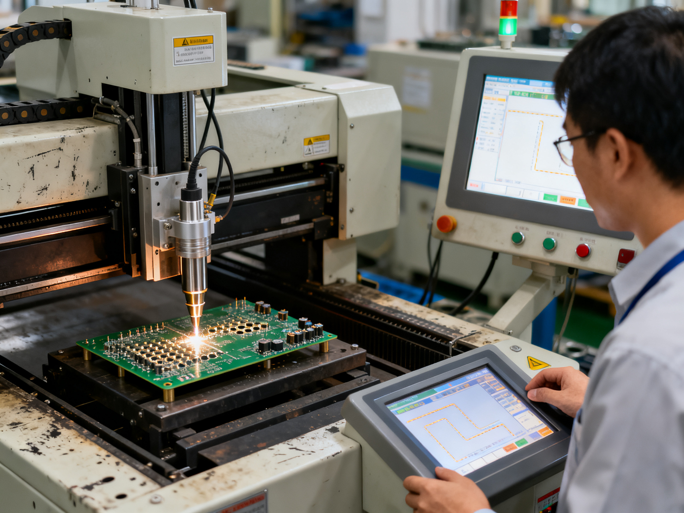
Here are the main selective soldering technologies you will encounter:
Mini-Wave Nozzle Soldering
This uses a small, shaped nozzle to create a localized solder wave just big enough for one or a few pads at a time. It’s fast, relatively affordable, and works well for mixed-technology boards. No custom masks required.
Laser Selective Soldering
The premium option. Lasers heat specific joints with incredible precision, and there is no physical contact with the board at all. This eliminates any risk of thermal stress on neighboring components entirely. Aerospace and medical manufacturers love this approach.
Robotic Soldering Systems
Automated arms that handle flux application, preheating, and solder deposition in a single programmable sequence. These inline systems balance speed with precision and work great for automotive electronics where volume still matters.
Programmable Solder Paths
Modern systems let you define exact solder paths in software. Change products without touching hardware. The software handles flux volume, preheat timing, and solder flow for each joint automatically.
From Our Experience: We use selective soldering for any board where wave soldering would put nearby SMT components at risk. Yes, it runs slower, but our defect rate on mixed-technology assemblies dropped from around 3 percent to under 1 percent once we switched. The math makes sense when you factor in rework costs.
Selective soldering shines brightest when your board has tight keep-out zones, heat-sensitive components, or a mix of through-hole and surface-mount technology that would be tricky to handle with a full wave.
| Term | What It Means |
|:—–|:————–|
| Keep-out zone | An area on the board where no soldering activity can occur |
| Mini-wave nozzle | A small solder nozzle that solders one small area at a time |
| Masking | Physical covering to protect areas from heat or solder (not needed with selective) |
| Programmable solder path | Software-defined sequence for where and how to solder each joint |
Wave Soldering vs Selective Soldering: Key Differences
The fundamental difference comes down to coverage. Wave soldering floods everything on the underside of your board in one pass. Selective soldering targets only specific joints or zones. That one difference shapes everything that follows: speed, cost, quality, and which applications each method handles best.
Process Coverage
Wave soldering works like a flood. Your PCB travels over a solder wave, and every exposed pad and through-hole underneath gets soldered at once. The upside is obvious: massive throughput for through-hole-heavy designs. The downside is that nearby surface-mount parts get exposed to heat and solder splash, which can damage sensitive components.
Selective soldering takes the opposite approach. A programmable nozzle or laser solders only the joints you specify. Everything else sits untouched. This protects sensitive parts but requires more programming time and runs significantly slower.
Throughput and Cost
Speed is where these two methods diverge most visibly. A wave soldering machine typically processes 200 to 1,000+ boards per hour depending on board size. Selective soldering usually handles 20 to 100 boards per hour per station, though multi-nozzle setups can push toward the higher end.
But raw speed does not always win on cost. Wave soldering needs custom pallets and fixtures costing $300 to $800 per setup, plus 1-2 weeks of lead time. For runs under 5,000 units or mixed-technology boards, those tooling costs can eat up the speed advantage fast. Selective soldering requires zero tooling, so you simply reprogram for each board variant.
Engineering Constraints
Board design matters more than preference here. Through-hole-heavy boards in stable, long production runs suit wave soldering well. Mixed assemblies with dense SMT components and tight keep-out zones around BGAs or QFNs often demand selective soldering.
Fixtures and pallets are wave’s biggest constraint. Every board variant needs physical tooling, which adds inventory overhead and slows changeovers. Selective systems handle high-mix production without physical tooling, though programming time varies.
Nitrogen use differs too. Wave systems need continuous N2 flow to control dross and oxidation in the solder pot. Selective systems apply solder sparsely and typically consume less nitrogen overall.
Which Method Wins?
The answer depends on your production profile. Wave soldering wins for high-volume through-hole runs with infrequent changeovers. Selective soldering wins for mixed assemblies and frequent product changes. Many SMT operations use both methods strategically depending on what they are building.
| Factor | Wave Soldering | Selective Soldering |
|:——-|:—————|:——————–|
| Throughput | 200 to 1,000+ boards per hour | 20 to 100 boards per hour |
| Precision | Broad coverage, all underside joints | Individual joint targeting |
| PCB Complexity | Simple to moderate THT-heavy | Complex mixed-technology |
| Fixture/Masking | Custom pallets required | No fixtures, software only |
| Labor Requirements | Higher setup, lower per-board | Lower setup, higher per-board |
| Defect Risk | 2 to 5 percent typical | Under 1 percent |
| Operating Cost | Lower per unit at high volume | Higher per unit, lower rework |
| Line Integration | Standard conveyor integration | Flexible station placement |
| Ideal Applications | Consumer connectors, automotive wire harnesses | Automotive ECUs, aerospace, medical devices |
Pro Insight: Wave soldering remains cost-effective for simple through-hole-heavy boards, but becomes riskier on dense mixed-technology assemblies. The defect rework costs often outweigh the speed gains when sensitive SMT components are nearby.
Citations:
- Selective Soldering vs Wave Soldering: Which Is Right for Your PCB?
- Selective Soldering vs Wave Soldering Comparison
- Wave or Selective Soldering: Which One to Choose and Why?
Wave Soldering Pros and Cons for High-Volume Manufacturing
Wave soldering has earned its reputation as the workhorse of through-hole assembly for good reason. It handles high volumes fast, keeps per-unit costs low, and the equipment ecosystem is mature and well-understood. But like any process, it has real limits that smart manufacturers factor into their decisions.
Where Wave Soldering Wins
When you’re running thousands of identical boards with mostly through-hole parts, wave soldering really shines. The throughput advantage is massive. A well-tuned line processes 200 to 1,000+ boards per hour depending on board size. That breaks down to pennies per joint at scale.
The technology itself is mature. Operators are easy to find, spare parts are plentiful, and the process window is well-documented. For products like consumer electronics connectors, automotive wire harnesses, and industrial control boards where most components are through-hole, wave soldering typically delivers the lowest cost per good board.
Where Wave Soldering Struggles
The problems show up fast when your board design gets complicated. Since wave soldering floods everything on the underside, any surface-mount parts nearby get exposed to 260-degree solder and thermal stress. Sensitive BGAs, QFNs, and moisture-sensitive components can fail or suffer reliability issues down the line.
You can mask these areas with pallets or fixtures, but that adds $300 to $800 per board variant and takes 1-2 weeks to produce. Dense SMT layouts also create bridging risks because pads sit close together. The solder pot itself consumes more flux and metal, and you deal with constant dross buildup that requires ongoing maintenance.
For mixed-technology boards or frequent changeovers, those tooling costs and changeover times eat into your throughput advantage fast. We see manufacturers get excited about 800 boards per hour, then realize they need three different fixtures and two weeks of setup for their product mix.
The Real Picture
For straightforward through-hole boards in long, stable production runs, wave soldering still makes the most sense in 2026. It delivers the best cost per joint when you’re building the same thing for months. But for complex mixed assemblies with sensitive components, the defect rework costs and fixture overhead often outweigh the speed gains. That’s why many SMT operations run both processes side by side, using each for what it does best.
Pro Insight: Wave soldering remains cost-effective for simple through-hole-heavy boards, but becomes riskier on dense mixed-technology assemblies. The defect rework costs often outweigh the speed gains when sensitive SMT components are nearby.
| Factor | Wave Soldering Advantage | Wave Soldering Limitation |
|:——-|:————————|:————————-|
| Throughput | 200 to 1,000+ boards/hour | Slows with complex boards |
| Per-Joint Cost | Lowest at high volume | Hidden fixture costs |
| SMT Compatibility | Works with proper masking | High defect risk without masking |
| Changeover Time | Fast for same board | 1-2 weeks for new fixtures |
| Defect Rate | Under 1% for simple boards | 2-5% for mixed assemblies |
| Equipment Maturity | Well-understood process | Older technology base |
Selective Soldering Pros and Cons for Complex PCB Assemblies
Selective soldering offers some serious advantages when your board design pushes traditional methods to their breaking point.
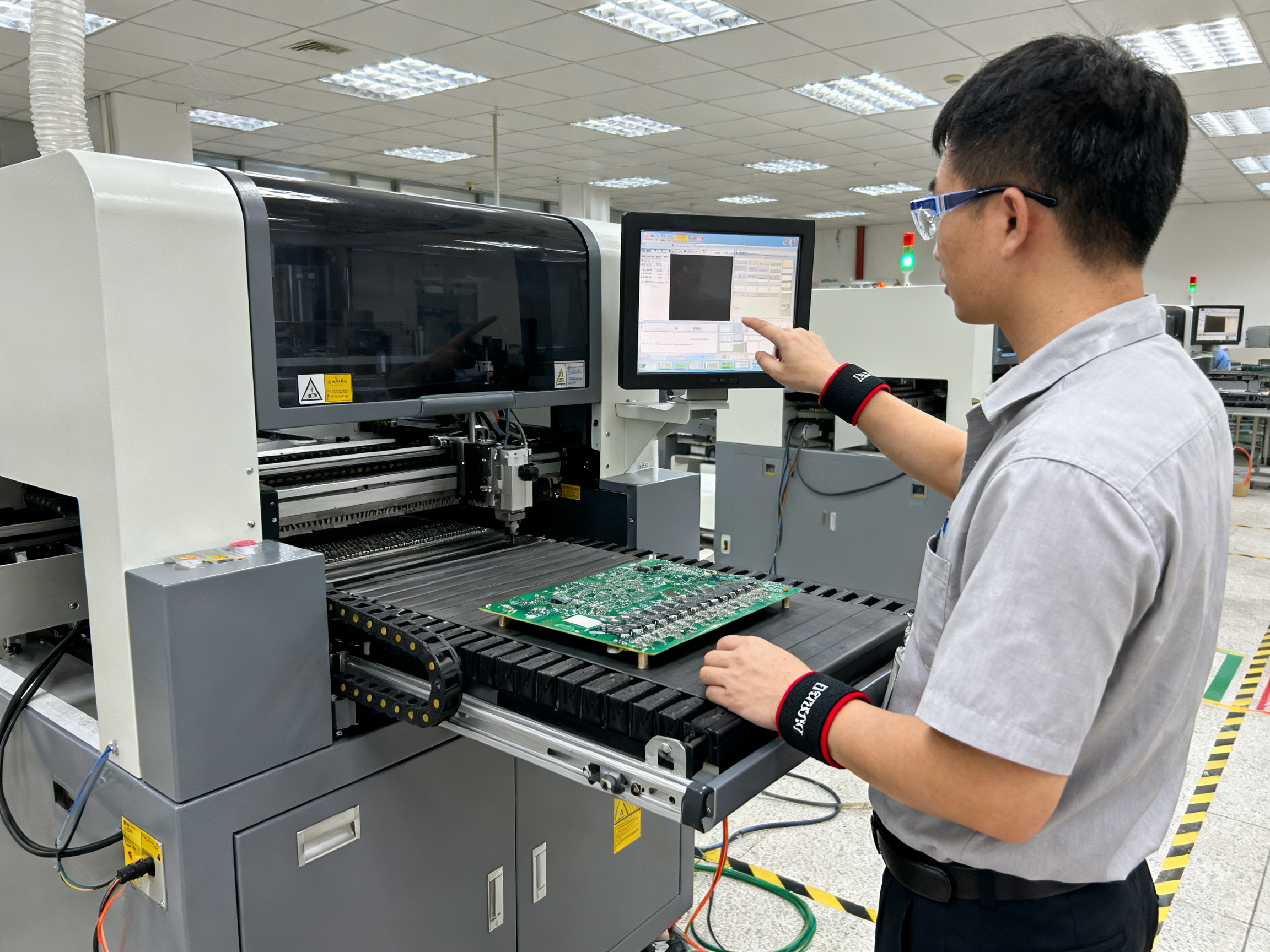
Where Selective Soldering Wins
Localized heat application is the biggest deal here. The solder only touches the joints you program it to touch. Everything else sits untouched at room temperature, which means your BGAs, QFNs, and moisture-sensitive components stay completely protected.
Precise solder delivery eliminates bridging and skips. When the nozzle targets one joint at a time, you get consistent fillet formation every single time. That consistency matters when you are building boards where every joint has to pass visual inspection.
No fixture costs. This one hits hard when you compare it to wave soldering. Wave systems need custom pallets at $300 to $800 per board variant. Selective soldering needs software changes, which cost nothing and take minutes instead of weeks.
Mixed SMT and through-hole assemblies suit this process perfectly. You can work around tight keep-out zones near surface-mount parts without worrying about heat or solder splash. The flexibility supports high-mix production where you run different board variants frequently.
Defect rates under 1 percent are typical for well-tuned systems. That drops rework costs significantly compared to wave soldering, which commonly sees 2 to 5 percent defects on complex mixed assemblies.
From Our Experience: We switched our automotive ECU production to selective soldering three years ago. The per-board cost went up, but our rework station basically gathered dust. The math worked out once we stopped counting rework labor and scrap boards.
Where Selective Soldering Falls Short
Speed is the obvious trade-off. Processing 20 to 100 boards per hour looks slow next to wave systems pushing 200 to 1,000 plus. For through-hole-heavy boards in long runs, that throughput gap hurts.
Equipment costs more upfront. The precision systems with multi-nozzle setups and advanced process control carry higher price tags than basic wave machines.
Programming takes time. Each joint needs its own parameters in the software. Complex boards with hundreds of through-hole parts need careful setup before the first board runs.
Nozzle access can be tricky on very dense layouts. If components sit too close together, the nozzle head may struggle to position itself correctly.
Maintenance adds up. Nozzles wear out, tips need replacing, and calibration checks keep the process in spec.
The Bottom Line
For complex mixed-technology assemblies in 2026, selective soldering often wins even with slower throughput. The defect reduction and protection of sensitive components outweigh speed concerns when the alternative is expensive rework or field failures.
| When Selective Soldering Makes Sense |
|:————————————|
| Tight keep-out zones around BGAs or QFNs |
| Mixed SMT and through-hole on same board |
| High-mix production with frequent changeovers |
| Aerospace, medical, or automotive Class 3 reliability |
| Dense layouts where wave bridging is likely |
| When Wave Soldering Still Wins |
|:——————————|
| Simple through-hole boards, high volume |
| Long stable runs with infrequent changeovers |
| Cost per board is the primary metric |
| Minimal SMT components nearby |
When to Use Wave Soldering, Selective Soldering, or Both
Think about your board. How many through-hole joints? How dense is the SMT layout? What’s your production volume like? Answer those three questions, and you’re already halfway to the right call.
Here’s a quick decision flowchart that works for most shops in 2026:
Board has mostly through-hole parts with few nearby SMT components?
  -> YES: Is your run over 5,000 units with infrequent changeovers?
       YES -> Use wave soldering
       NO  -> Calculate fixture costs vs. volume
  -> NO:  Does board have BGA/QFN near THT pads or tight keep-out zones?
       YES -> Use selective soldering
       NO  -> Mixed-technology assembly with frequent product changes?
            YES -> Use selective soldering
            NO  -> Consider a hybrid line using both
Go with wave soldering when:
Your board has mostly through-hole parts, runs are long and stable (same product for hours), and you want the lowest cost per joint. Consumer electronics connectors, automotive wire harnesses, and industrial control boards fit this profile perfectly. The math works out when you’re building 50,000 identical units and your changeover time stays low.
Go with selective soldering when:
Your assembly mixes SMT and through-hole parts, you have tight keep-out zones around BGAs or QFNs, products change frequently, or you’re building aerospace or medical devices where defect rates matter more than speed. Yes, the slower throughput hurts. But your rework station will thank you.
Use both when it makes sense:
Here’s what a lot of manufacturers do. They run wave soldering for straightforward through-hole products at high speed. Then they dedicate selective soldering stations for complex mixed-technology boards or product families that see frequent design changes. This hybrid approach handles anything that doesn’t fit neatly into one category.
The real answer in 2026 isn’t choosing one method or the other. It’s knowing which process fits each product on your line, then building your workflow around that flexibility.
From Our Experience: We use a simple scoring system with our production planners. Five points for wave-suitable features (mostly THT, simple layout), five points for selective-suitable features (mixed tech, sensitive parts, high-mix). The higher score wins. Takes 10 minutes per new product, saves hours of arguments later.
How to Choose Between Wave Soldering and Selective Soldering
So you’ve got the specs. You know the differences. Which one belongs on your production floor?
Here’s a quick decision framework for 2026. Run your board through these six questions:
1. Board Complexity
Mostly through-hole with few nearby SMT parts? Wave soldering handles it. Mixing BGAs, QFNs, and tight keep-out zones near THT pads? You need selective soldering.
2. Volume and Takt Time
Need 500+ boards per hour with stable, long runs? Wave wins on speed. High-mix production with frequent changeovers? Selective wins because there’s zero fixture cost.
3. Defect History
Current rework rate sitting at 2 to 5 percent? Switching to selective typically drops that to under 1 percent. The rework labor savings often justify the slower speed.
4. Total Cost of Ownership
Factor in machine price, energy, nitrogen, solder, flux, pallets, maintenance, programming, and rework. For runs under 5,000 units, selective eliminates $300 to $800 per fixture costs entirely.
5. Compliance Requirements
Aerospace, medical, or automotive Class 3 work? Both methods meet IPC-A-610J and J-STD-001J, but selective’s programmable recipes make audit trails simpler.
6. Line Integration
Wave drops into standard conveyors. Selective needs its own station, MES data connection, and AOI linkage. Floor space matters here.
From Our Experience: We use a simple scoring system with our production planners. Five points for wave-suitable features (mostly THT, simple layout), five points for selective-suitable features (mixed tech, sensitive parts, high-mix). The higher score wins. Takes 10 minutes per new product, saves hours of arguments later.
| Factor | Wave Soldering | Selective Soldering |
|:——-|:—————|:——————–|
| Throughput | 200 to 1,000+ boards/hour | 20 to 100 boards/hour |
| Fixture Cost | $300 to $800 per variant | Zero, software only |
| Defect Rate | 2 to 5 percent typical | Under 1 percent |
| Best For | Simple THT-heavy boards | Mixed-tech, high-mix, Class 3 |
The quick test: Can your board run through a wave without damaging nearby SMT components? If yes, wave probably wins on cost. If no, selective soldering is the safer bet.
Testing and Quality Assurance for Soldered Joints
So you have got your boards through the soldering process. Now what? How do you actually verify that every joint is good and ready for the field?
Quality assurance in wave and selective soldering goes beyond a quick visual inspection. For high-reliability applications, you need a structured approach that catches defects before they reach your customers.
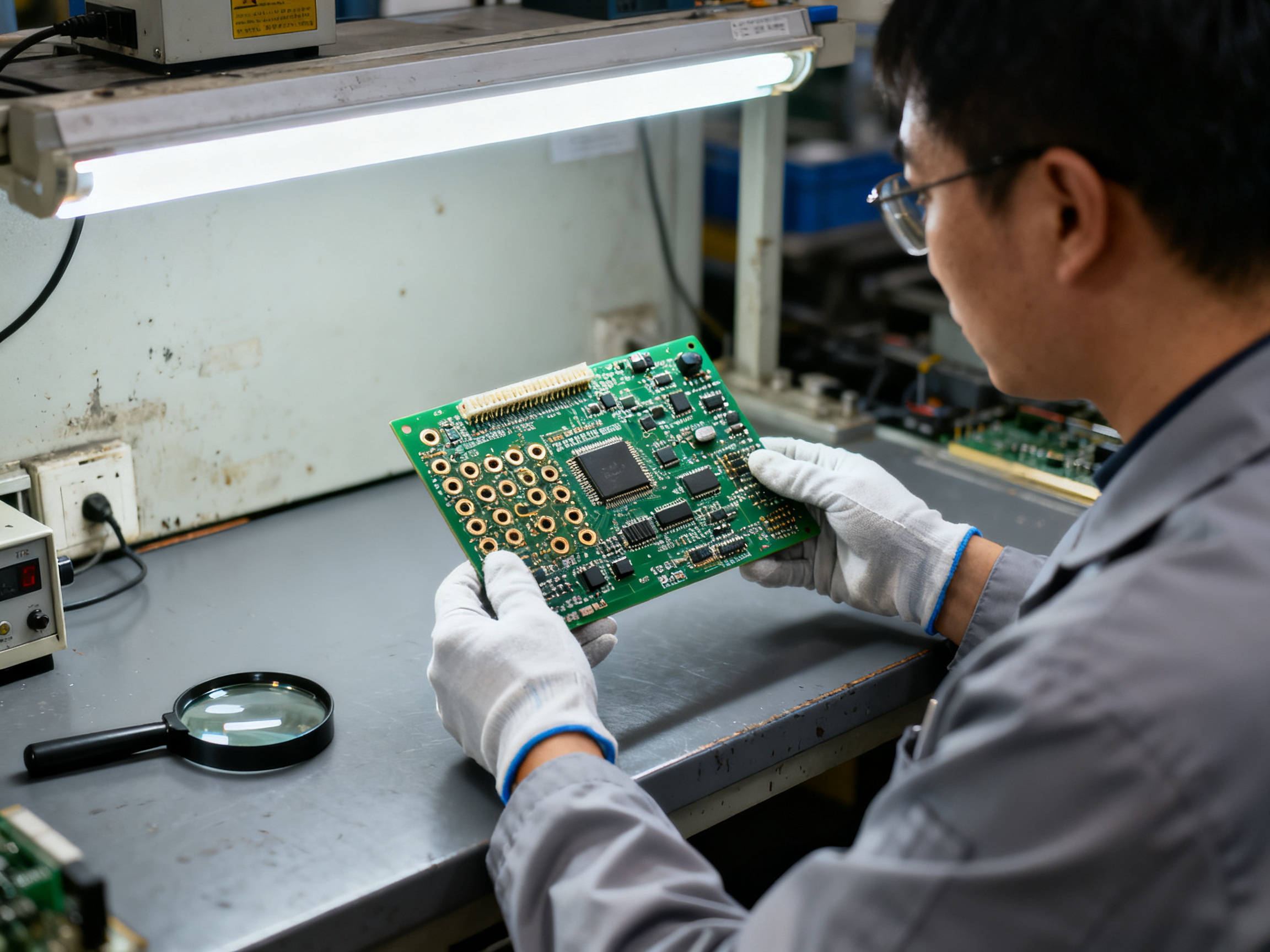
Visual Inspection Fundamentals
The first line of defense is always visual inspection. Train your operators to look for the classic signs of good joints: shiny fillets, proper wetting around leads, and complete hole fill. IPC-A-610J defines exactly what Acceptable, Target, and Defect conditions look like for each joint type.
For wave-soldered boards, focus on the solder side. Look for bridging between adjacent pads, icicles hanging off joints, and any signs of insufficient fill where the solder did not pull up through the hole completely. Selective soldered joints should show clean, well-formed fillets without excessive solder or voids.
Automated Optical Inspection
For production volumes, automated optical inspection (AOI) systems catch defects faster and more consistently than manual inspection. Modern AOI cameras can identify bridging, insufficient solder, misalignment, and component placement issues at speeds that keep up with production lines.
AOI works particularly well for selective soldering where joint consistency is high. The system learns what a good joint looks like and flags anything outside tolerances automatically.
X-Ray and Cross-Section Analysis
Some defects hide below the surface. BGAs, QFNs, and other bottom-terminated components hide their solder joints from visual inspection entirely. For these, X-ray inspection is essential.
X-ray reveals voiding inside joints, insufficient fill, and alignment problems that would otherwise go unnoticed. Cross-section analysis takes this further by cutting sample boards and examining the joint microstructure under a microscope. This is typically reserved for qualification builds and failure analysis rather than production inspection.
In-Circuit Testing
In-circuit testing (ICT) verifies that each component on the board is present, oriented correctly, and electrically connected properly. ICT catches missing components, solder bridges that create short circuits, and open circuits from insufficient fill.
Functional testing goes a step further by actually exercising the board is circuitry to verify it behaves as expected. This catches issues that ICT might miss, like marginal joints that pass electrical testing but fail under thermal stress.
Building an Inspection Strategy
Not every board needs the same level of inspection. Match your inspection intensity to your reliability requirements.
For consumer products with short expected lifespans, visual inspection plus AOI is usually sufficient. For automotive, medical, or aerospace applications, you need X-ray inspection for hidden joints, plus functional testing under thermal cycling conditions to verify long-term reliability.
Document your inspection criteria in your work instructions. Make sure operators know exactly what to look for and what action to take when they find a defect. A clear escalation path ensures problems get addressed before boards ship.
From Our Experience: We run first-article inspection on every new board layout, including X-ray on hidden joints. Once we verify the process is stable, we switch to statistical process control with periodic sampling. This balances quality assurance with production throughput. Our escaped defect rate stays below 0.1 percent with this approach.
Pro Tip: Keep defect data by board revision, operator, and production date. When you see defect trends, you can trace them back to root causes quickly. A spike in bridging on one shift might point to a conveyor alignment issue. Patterns matter.
| Inspection Method | What It Catches | Best For | Limitations |
|:——————|:—————-|:———|:————|
| Visual inspection | Bridging, icicles, cold joints, alignment | All production | Human variability, misses hidden joints |
| AOI | Surface defects, component placement | High-volume production | Cannot see under BGAs/QFNs |
| X-ray inspection | Hidden joint defects, voiding | BGA/QFN assemblies, high reliability | Cost, slower throughput |
| ICT | Electrical opens and shorts | Production screening | Requires test fixtures |
| Functional testing | Real-world performance | Final verification | Does not pinpoint defects |
Quality assurance is not optional in electronics manufacturing. It is what separates boards that work reliably for years from boards that fail in the field and damage your reputation. Invest in the right inspection methods for your reliability class, and build the data feedback loops that let you improve continuously.
Citations:
- IPC-A-610J Acceptability of Electronic Assemblies
- X-Ray Inspection for Electronics Manufacturing
- In-Circuit Testing: A Complete Guide
- AOI vs X-Ray Inspection for PCB Assembly
Expert Recommendation: Match the Soldering Method to Product Risk, Not Just Volume
Here’s the bottom line after all the technical details, defect rates, and cost breakdowns. Wave soldering and selective soldering aren’t competing against each other. They’re complementary tools that serve different purposes on your production floor.
Choose wave soldering if:
- Your boards are through-hole-heavy with minimal nearby SMT components
- Production runs stay stable for weeks or months at a time
- Volume hits 5,000+ units per run
- Cost per joint is your primary metric
Choose selective soldering if:
- Your assemblies mix dense SMT with through-hole parts
- You have BGA, QFN, or other heat-sensitive components near THT pads
- Product changeovers happen frequently
- Defect rework costs are eating into your margins
- You’re building for automotive, aerospace, or medical reliability standards
Consider both if:
- Your product mix spans simple connectors to complex mixed-technology boards
- You want maximum flexibility without sacrificing throughput on high-volume SKUs
The real question isn’t which method is better. It’s which method fits your specific board families, your reliability requirements, and your production schedule right now.
So what’s your next move? Audit your current PCB families and map out your defect history by product line. Calculate the total cost of ownership for each method including rework labor, scrap rates, and fixture inventory. Run sample boards through both processes if you can. And talk to an SMT equipment specialist who understands your industry before signing anything.
The right choice today might look different two years from now as your product mix evolves. Build that flexibility into your decision from the start.