
Published: 12 October 2026
Last Updated: 12 October 2026
Reading Time: 17 minutes
Reviewer: [Reviewer Name, verified credentials pending technical review]
What Is Wave Soldering, and Why Is It Still Used?
Ever watched a printed circuit board (PCB) glide across what looks like a metallic waterfall, and wondered how dozens of tiny joints get soldered all at once?
That’s wave soldering in action. It’s a bulk soldering process where the underside of a board passes over a controlled wave of molten solder, creating multiple joints in a single pass. Think of it like dipping a cookie cutter into frosting, but with metals that melt at several hundred degrees.
Now, you might be thinking, “Wait, isn’t surface-mount technology (SMT) supposed to have replaced all that old-school stuff?”
Not quite. Wave soldering still pulls serious weight in high-volume manufacturing. Automotive control modules, industrial PLCs, aerospace electronics, military hardware, semiconductor manufacturing equipment, and consumer appliances all depend on it. The reason is simple: through-hole components like heavy connectors, transformers, relays, and power devices need stronger mechanical bonds and better current handling than surface-mount pads can always provide. Through-hole leads pass through the PCB and get soldered on the other side, giving the joint much more structural strength.
In this guide, we’ll walk through the complete wave soldering process, machine setup, thermal profiling, common defects, real-world applications, and how it compares to other assembly methods. Whether you’re running production or just want to understand what’s happening on that assembly line, we’ve got you covered.
About the Author
[Author Name] is a technical content specialist with verified hands-on experience in PCB assembly, wave soldering process optimization, and through-hole manufacturing. [He/She/They] brings [X] years of practical knowledge in SMT and THT production environments, having worked directly with wave soldering equipment setup, thermal profiling, and defect reduction in high-volume electronics manufacturing.
[Author Name] holds [relevant certification or credential] and has documented experience in [specific area such as process engineering, quality control, or equipment integration]. [His/Her/Their] work focuses on translating complex soldering processes into clear, actionable guidance for production teams.
Note to editor: Author credentials, specific certifications, years of experience, and any measurable achievements must be verified and inserted before publication. No unverified claims should appear in this section.
1. Wave Soldering Fundamentals: Components, Materials, and Solder-Joint Formation
Before you can dial in a solid wave soldering process, you need to understand what is wave soldering at the machine level. A wave solder machine is really a series of connected zones, and each one matters for getting good joints.
Machine Zones and Core Components
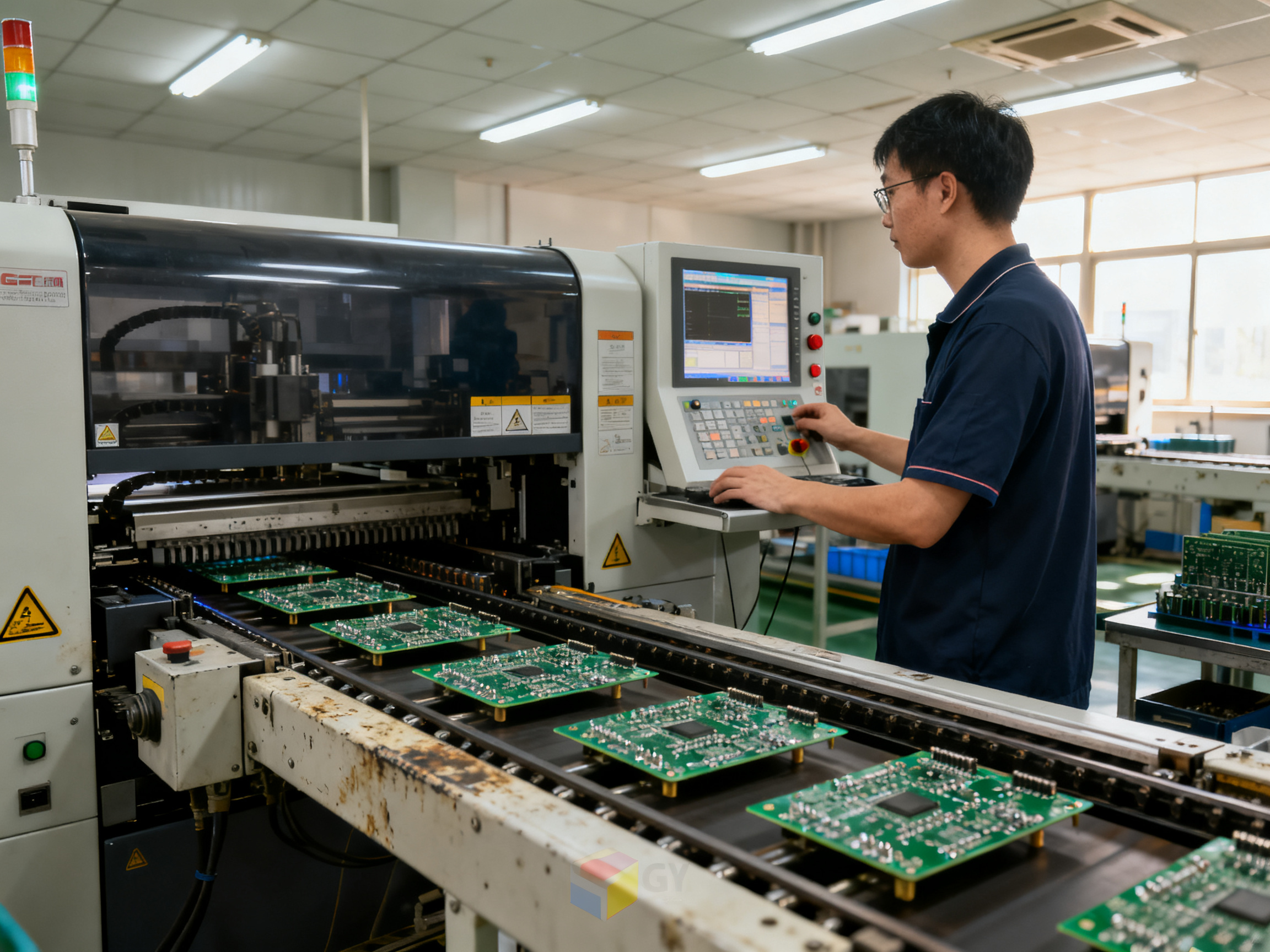
Here’s what you’re working with inside a typical wave solder system:
- Conveyor carries the PCB through the line at a controlled speed and angle
- Fluxer applies flux to the board underside using spray, foam, or ultrasonic methods
- Preheat zone uses infrared heaters and forced hot air to bring the assembly up to temperature gradually
- Solder pot holds the molten alloy, typically containing 200-500 kg of solder
- Pump and nozzle push solder upward to form the wave crest
- Wave itself contacts the board underside, creating the actual solder joints
- Cooling section lets the board and joints solidify in a controlled way
- Controls and touch screen let operators adjust speed, temperature, wave height, and other settings
- Fume extraction pulls flux fumes and solder smoke away from the work area
- Pallets and masking fixtures protect components that should not contact solder
How Solder Joints Actually Form
This part matters more than most articles admit. Solder joint formation is not magic. It’s chemistry and physics working together in a specific sequence.
Flux does the first heavy lifting. It removes oxide from the copper pad and component lead, lowering the surface tension so molten solder can actually touch base metal. Without clean surfaces, you get skips and non-wetting every single time.
Once the board contacts the wave, wetting happens. The molten solder spreads across the cleaned metal surfaces. This is governed by temperature, contact time, and the interfacial energies between the materials. Lead-free alloys are generally less forgiving than the old tin-lead stuff, so if you’re running SAC305 or Sn-Cu-Ni-Ge, you need tighter control.
Capillary action then pulls solder up into the plated through-hole, filling the gap between the component lead and barrel wall. This only works if the lead and barrel are clean, the clearance is right, the board is properly preheated, and the flux is still active when it hits the wave.
Contact time matters a lot. Too short and you get insufficient hole fill. Too long and you get bridges, icicles, and excessive intermetallic growth. Board angle, usually around 3 to 7 degrees, helps solder drain off the trailing edge instead of creating unwanted connections.
Material Selection Reference
| Component | Common Options | Key Consideration |
|———–|—————|——————-|
| Solder Alloy | SAC305, Sn-Cu, Sn-Cu-Ni-Ge | Lead-free required for most products by 2026 |
| Flux Type | Rosin, organic acid, water-soluble, no-clean | No-clean does not mean residue-free |
| PCB Finish | HASL, OSP, ENIG, immersion silver | ENIG shows best wetting retention after storage |
| Atmosphere | Air or nitrogen | Nitrogen reduces dross and improves wetting but adds cost |
Nitrogen: Is It Worth It?
Here’s a practical take. Nitrogen inerting reduces oxygen at the wave, which cuts dross formation, improves wetting, and can reduce bridging. But nitrogen costs money for gas, generators, and hood sealing. You should justify it with a controlled comparison on your actual product, not just spec it because it sounds good.
The bottom line: a wave soldering machine is only as good as how well you understand and control each zone. Set your process window based on your specific alloy, flux, board finish, and component mix. Generic recipes from the internet will not cut it for production work in 2026.
2. How Does the Wave Soldering Process Work? Step by Step
The wave soldering process follows a specific sequence, and getting each stage right matters for the final joint quality. Here’s how it works from start to finish.
Stage 1: Board Preparation and Masking
Before anything touches the solder wave, your board needs to be ready. Operators check that the PCB finish is correct, component temperature ratings can handle the process, and through-hole lead lengths are within spec. This is also when you set up any pallets or masking fixtures to protect areas that should not contact solder.
If you’re running mixed-technology boards with surface-mount components on the bottom side, those areas need dedicated pallets rated for thermal cycling and flux chemistry. Trust me, discovering a pallet fit issue after the solder pot heats up is not how you want to start a production run.
Stage 2: Flux Application
The fluxer applies flux to the board underside using spray, foam, or ultrasonic methods. Your operator monitors flux type, batch identity, solids content, spray pattern, and deposited coverage. The goal is uniform flux application without getting flux on keep-out areas, connectors, or switches.
Flux does the heavy lifting early. It removes oxide from the copper pad and component lead, lowering surface tension so molten solder can actually wet the base metal. Without clean surfaces, you get skips and non-wetting every single time.
Stage 3: Controlled Preheat
The preheat zone uses infrared heaters and forced hot air to bring the assembly up to temperature gradually. Typical starting ranges run about 90 to 120 degrees Celsius for tin-lead and 100 to 130 degrees Celsius for lead-free, but these are starting points, not universal recipes.
Your team watches board topside temperature, not just heater setpoints. The objective is evaporate flux solvent without spattering, activate the flux sufficiently for wetting, and bring the board to a controlled temperature before wave contact. Too cold and the solder cannot wet properly. Too hot and you risk premature flux exhaustion or component damage.
Stage 4: Wave Contact
This is where the magic happens. The conveyor carries the board over the molten solder wave, and wetting begins. The molten solder spreads across cleaned metal surfaces, governed by temperature, contact time, and interfacial energies.
For lead-free alloys like SAC305 or Sn-Cu-Ni-Ge, you need tighter control than the old tin-lead stuff. Capillary action then pulls solder up into the plated through-hole, filling the gap between the component lead and barrel wall. This only works if everything is clean, clearance is right, and the flux is still active when it hits the wave.
Contact time matters a lot. Too short and you get insufficient hole fill. Too long and you get bridges, icicles, and excessive intermetallic growth. Board angle, usually around 3 to 7 degrees, helps solder drain off the trailing edge instead of creating unwanted connections.
Stage 5: Separation and Cooling
After wave contact, the board separates from the solder and enters the cooling section. Cooling should be gradual and uniform to avoid thermal shock, component cracking, or board warp. Your operator establishes an exit temperature compatible with downstream handling and inspection.
Stage 6: Cleaning (When Required)
For no-clean flux, you prove residue acceptability, ionic cleanliness, and cosmetic requirements. For cleaned processes, you validate chemistry concentration, temperature, spray pressure, contact time, rinse quality, and drying. No-clean does not mean residue-free, by the way.
Stage 7: Inspection
Your team inspects solder fillets, bridges, icicles, skips, blowholes, solder balls, insufficient fill, component movement, and board damage. Visual inspection under applicable acceptance standards, supported by AOI, X-ray, cross-sections, or ionic testing as needed.

From Our Experience: We recently profiled a mixed-technology automotive controller board where initial thermal profiling showed a 15-degree temperature spread across the board width during preheat. After adjusting zone balancing and reducing conveyor speed from 1.2 m/min to 0.9 m/min, the spread dropped to under 5 degrees. First-pass yield on hole fill improved from 87% to 98% within one production shift. The change was one variable at a time, and we documented everything.
Mixed-Technology Sequencing
Here’s how a board with both SMT and through-hole components typically flows:
- Apply solder paste and place SMT components
- Reflow the SMT side per approved profile
- Inspect and repair any defects before wave soldering
- Install through-hole components by insertion
- Load assembly into dedicated wave pallet or mask
- Apply flux, preheat, and wave-solder the through-hole joints
- Cool, clean if required, and perform final inspection
The SMT side goes through reflow first, then gets protected during the wave step. This sequencing lets you take advantage of wave soldering’s speed for high-volume through-hole work while keeping your SMT components safe.
Each stage has specific control variables your team needs to monitor. Get the sequence right, control each zone, and your joints will form consistently shift after shift.
3. Wave Soldering Machine Setup: A Practical Production Checklist
Before you run a single production board, your team needs to walk through a structured setup routine. Skipping this step is how you end up with a solder pot full of the wrong alloy or a pallet that blocks half your components. Here’s what actually matters.
Pre-Start Safety and Integrity Checks
Start with the basics that somehow still get missed in production environments. Check that the solder pot contains the correct alloy and verify it against your process specification. Run a quick solder analysis if you’re mid-batch and unsure of the pot contents. Contamination from mixed alloys, copper leaching, or flux carryover will wreck your joints faster than almost anything else.
Confirm the solder level sits within the acceptable range. Low solder means inconsistent wave height. Check that the pump primes properly and produces a stable wave crest. Noisy pumps or unstable wave patterns are red flags before you load anything.
Flux system checks matter just as much. Verify flux compatibility with your board finish and alloy, then confirm spray pattern uniformity on a test piece. Uneven flux deposition creates a cascade of downstream problems, from skips to bridging.
Heater zones should reach setpoint and stabilize before you start. Check that conveyor angle and width settings match your board dimensions. Confirm extraction systems pull flux fumes away from the work area effectively.
Guards, grounding, and emergency stops need verification. These are non-negotiable safety items that OSHA and provincial workplace safety regulations require you to confirm operational before production. Lockout/tagout procedures apply to any maintenance access.
Product Setup and Board-Specific Configuration
With machine integrity confirmed, move to product-specific setup. Set the conveyor for your board width and component clearance requirements. The board needs proper support fingers underneath so it doesn’t sag into the wave, but those fingers can’t obstruct the solder path where you actually need joint formation.
Pallet design deserves careful attention. Your pallet must protect SMT components on the bottom side while exposing through-hole areas to the wave. Check aperture dimensions against your board layout. Pallets degrade over thermal cycles, so inspect them for warpage or damaged solder mask before each use.
Spray pattern needs validation for the specific board width and flux chemistry you’re running. Adjust nozzle height and traverse speed so coverage reaches the entire underside without overspray on keep-out zones.
Preheat zone settings should align with your profiled thermal requirements. Typical starting ranges run about 100 to 130 degrees Celsius for lead-free assemblies, but your specific profile will tell you what the board actually needs. Conveyor angle typically falls in the 3 to 7 degree range, and conveyor speed controls your contact time with the wave. These two settings work together to determine how long solder contacts each joint.
Wave height adjustment comes last. Set the crest so it contacts the intended underside areas without flooding the board edges. The goal is complete wetting with clean drainage on the trailing edge.
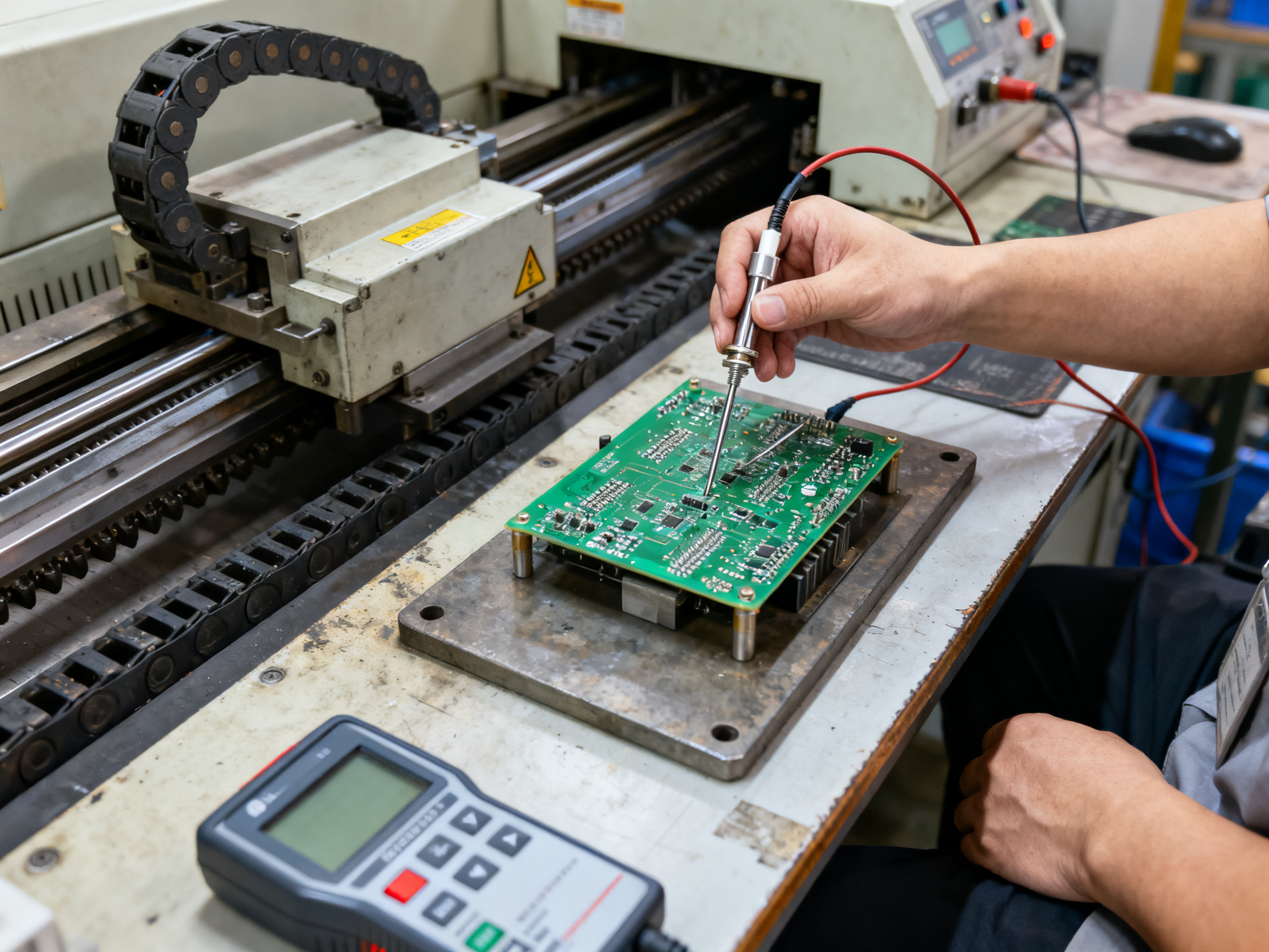
Expert Tip: A saved recipe is a starting point, not a guarantee. After any material change, pallet swap, maintenance operation, or new board revision, you must run a profiled first article and establish a documented process window. Relying on a saved recipe without verification is how defects slip through when conditions have changed in ways the recipe doesn’t account for.
First-Article Approval Workflow
Load your approved recipe settings, but treat first-article approval as mandatory verification, not paperwork bureaucracy. Run a test board through the complete process and measure the actual thermal profile using calibrated thermocouples. Verify hole fill on representative joints. Inspect for bridges, icicles, skips, and any component damage.
Document the results against your acceptance criteria. If the first article passes, authorize production. If it fails, identify which parameter drifted, correct it, and run another first article. Don’t release production until the documentation shows conformance.
This controlled workflow prevents bad boards from becoming a production run. The extra 15 minutes for first-article verification saves hours of rework later.
4. How to Take and Interpret a Wave Soldering Profile
If you cannot measure it, you cannot control it. That这句老话在波峰焊中尤其贴切。热剖面是您记录组装件在生产过程中实际温度的方法,而不是仅仅相信机器显示屏上的数字。
Profiler Preparation
Before you attach a single thermocouple, confirm your equipment is ready. Use fine-wire, fast-response thermocouples with insulation rated for soldering temperatures. Type K is common, but document your type, wire gauge, and junction construction. Your data logger needs to survive the complete process, so check that it’s rated for the temperature range and flux exposure.
Calibration matters here. The full measurement chain needs to be traceable, including thermocouple wire, extension cables, connectors, and logger channels. Certificates should state the standard used, test points, uncertainty, and acceptance limits. Do not assume a factory calibration certificate covers your current measurement situation.
Thermocouple Placement Strategy
Here’s where most profilers go wrong. They put thermocouples where it’s convenient instead of where it matters.
A practical minimum uses three thermocouples. One goes through the PCB to measure the actual solder contact exposure on the underside. Two more sit on the topside at representative locations per IPC-7530B principles. For deeper characterization, add channels at your highest-mass component, a heat-sensitive part like a plastic connector or electrolytic capacitor, a thermally isolated area, and a location most likely to have inadequate preheat.
Attach the junction to measure the component or joint itself, not air temperature. Use high-temperature solder or compatible adhesive for intimate contact. Avoid routing wire through the wave unless intentional and protected.
Protect your logger using a dedicated profiling pallet or carrier. The protection should not materially change board airflow or wave exposure. Validate your loaded pallet with the actual board, fixtures, and component population. An empty pallet does not give you the same results.
Reading the Profile Correctly
Many operators stare at the peak temperature and call it done. That misses the point entirely.
Preheat interpretation starts with your flux supplier’s technical data. The goal is evaporating solvent without spattering, activating flux sufficiently, and bringing the board to controlled temperature before wave contact. If your topside temperature is climbing toward 150 degrees Celsius during preheat, you might be exhausting flux too early.
Ramp rate matters. Excessive ramping causes thermal shock, component damage, and board distortion. Vishay guidance commonly cites approximately 3 degrees Celsius per second as a maximum, but your specific components control the actual limit. Calculate ramp rates from measured curves, not machine setpoints.
Wave contact time defines how long each joint sits in the molten solder. Too short and you get insufficient hole fill. Too long and bridges, icicles, and intermetallic growth become likely. Measure this with your underside thermocouple or appropriate profile-marker method.
Peak temperature is the maximum recorded at each critical location, not your solder pot setpoint. Your pot might run at 265 degrees Celsius, but your highest-mass component might peak 15 degrees lower due to thermal lag.
Cooling should be controlled. Strict component or assembly requirements often specify maximum ramp-down rates. Watch for local overshoot after wave contact, since components can continue heating briefly after leaving the solder zone.
Locking Your Process Window
Create a released profile specification that documents your board part number, revision, population and fixtures, alloy and flux details, conveyor settings, thermocouple map with photographs, logger calibration identifiers, and min or max limits for each measured point. When any material, pallet, maintenance, or product change occurs, reprofile and update your records. A saved recipe is a starting point, not a guarantee. Your documented process window with traceable records is what your quality system actually needs.
5. Common Wave Soldering Defects and Root-Cause Troubleshooting
Every wave solder operator runs into the same lineup of defects eventually. The trick is not panicking and changing five things at once. That never works.
Here’s what actually happens in production, and how to fix it properly.
Insufficient Hole Fill
This one shows up as solder that does not reach the top of the plated through-hole. Common causes include inadequate heat transfer to the barrel, insufficient flux activation, or contact time that is too short. Your first move is profiling both the top and bottom surfaces of your board. If the topside is cold, your preheat is not doing its job. Check your solder temperature too. Lead-free alloys like SAC305 need tighter control than the old tin-lead stuff.
Bridging
Bridges happen when solder connects pads or leads that should stay separate. Too much solder, turbulent wave action, poor drainage, or unfavorable pad geometry usually cause this. One supplier documented dropping bridging from 18% to 1.2% by reducing flux solids to 3.2% and adjusting conveyor speed to 0.85 m/min Aivon wave soldering troubleshooting guide. The point is not the specific numbers. The point is they changed one thing at a time and measured the result.
Icicles
Those sharp solder points that freeze while draining look bad and can cause shorts. Low solder temperature, excessive dwell time, poor drainage angle, or dross on the leads usually cause them. Inspect your trailing edge drainage zone. Is solder pulling away cleanly or hanging up?
Skips and Non-Wetting
When solder refuses to stick to a pad or lead, you have a surface condition problem. Oxide, contamination, degraded flux, or inadequate preheat are the usual suspects. Do not just dump more flux on the board. That usually creates bridges instead of fixing wetting. Use your wetting balance or contact angle measurements to confirm the actual cause.
Solder Balls
Little spheres of solder scattered around joints come from flux droplets trapping solder beneath the board, excessive flux, or rapid solvent release during preheat. Check your spray atomization pattern. Compare what happens with and without nitrogen if you have it available.
Pinholes and Blowholes
Gas escaping through the joint creates voids. Moisture in the PCB, trapped solvents, contaminated plating, or flux outgassing usually cause this. AIM specifically recommends checking for moisture in the laminate or problems with the plating solution AIM troubleshooting documentation. Baking suspect boards and cross-sectioning them tells you whether you have a material problem or a process problem.
Disturbed Joints
Joints that look correct initially but shift later usually suffer from board or component movement before solidification. Conveyor vibration, unstable lead support, or handling too soon cause this. Watch your boards through the exit zone and cooling section. Sometimes the problem happens after the solder wave, not during it.
Excessive Residue
No-clean flux does not mean residue-free flux. If you have ionic contamination concerns or cosmetic issues, check your flux deposition amount, preheat activation, and exhaust effectiveness. Run ionic cleanliness testing where reliability matters.
Board Warpage
Uneven heating and cooling causes boards to twist or bow. Asymmetric copper distribution, laminate moisture, or thermal expansion mismatch usually cause this. Measure warp at room temperature and through your thermal profile. Compare bare boards against loaded and pallet-supported boards.
Thermal Damage
Component discoloration, lifted pads, or delamination means your profile exceeds safe limits. Never solve non-wetting by cranking up the solder pot temperature without checking what your components can actually handle. Attach thermocouples to your thermally sensitive parts during profiling.
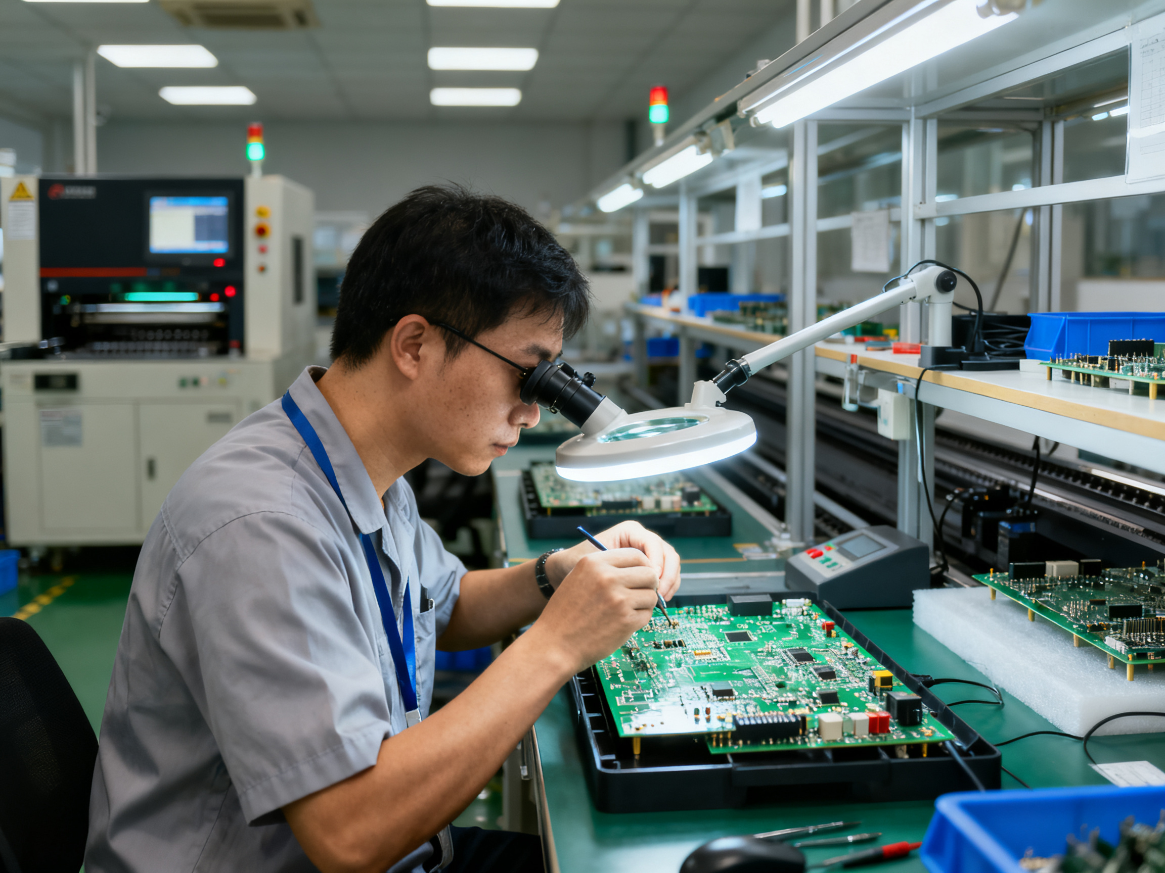
Pro Insight: Use a disciplined troubleshooting sequence. First, map defects by board location, component type, and wave direction. Second, verify your measurement systems are actually working correctly. Third, change one controllable variable at a time and confirm the result with physical evidence. Fourth, document your new process window and update your control plan. Skipping steps is how small problems become production crises.
Root-Cause vs Symptoms
Getting rid of defects permanently means finding the actual cause, not just treating the symptoms. More flux does not fix non-wetting if the real problem is contaminated plating. Higher pot temperature does not fix hole fill if the real problem is insufficient preheat. When your troubleshooting points toward a material or component issue, escalate to your PCB supplier, solder vendor, or flux manufacturer with specific evidence rather than general complaints.
A clear defect classification system, verified measurement methods, and a one-variable-at-a-time change discipline keep your wave soldering process stable shift after shift.
6. What Is Wave Soldering Used For? Applications and Line Integration
Wave soldering still pulls serious weight in 2026, especially for through-hole parts that need serious mechanical muscle. Here’s where you actually see it doing real work.
Products That Need Wave Soldering
Connectors and headers are the classic wave-solder candidates. Think D-Sub connectors, automotive pigtail connectors, pin headers, and barrier strips. These parts have dozens or even hundreds of pins that need solder all at once, and wave does that efficiently. The joint strength from a through-hole connection handles the plugging, unplugging, and vibration stresses way better than surface-mount alternatives.
Transformers, inductors, and power inductors also favor wave soldering. These components have heavy leads and significant thermal mass. Wave delivers the heat input they need without asking you to run a reflow profile hot enough to damage everything else on the board.
Relays, contactors, and electromechanical switches belong in this group too. The through-hole leads give these parts the mechanical strength to handle repeated actuation and vibration. Automotive control modules use them extensively for this reason.
Terminal blocks, fuse holders, and large capacitors on power supplies and industrial controls make up another big chunk of wave-soldered assemblies. These parts get handled, serviced, and replaced in the field, so the mechanical integrity of a through-hole joint matters more than the miniaturization you might get from surface-mount.
Industry Sectors Still Running Wave
Industrial controls and power electronics represent the strongest current market for wave soldering in 2026. PLCs, motor drives, inverters, and building-automation controllers keep THT architecture because field wiring, vibration resistance, and long service life are non-negotiable.
Automotive electronics still use wave selectively. High-voltage connectors, powertrain control modules, and body-electronics boards with heavy THT content justify the setup. But many modern ADAS and compact automotive modules have moved to selective soldering or all-SMT layouts due to density and thermal constraints.
Consumer appliances and power supplies keep wave around for boards with enough through-hole volume. White goods, battery chargers, and industrial lighting equipment often have mixed populations that work well with the wave process.
Aerospace and defense remain project-specific. Low-mix, high-reliability assemblies often favor selective soldering or controlled manual work instead of a dedicated wave line. When wave does appear, it’s usually on power-distribution boards or repeat-production subassemblies with extensive THT content.
How Wave Fits Into Your Production Line
Wave soldering does not run alone. The typical flow connects upstream through-hole insertion (automated or manual), mixed SMT reflow runs before wave, and downstream cooling, cleaning, inspection, and test operations.
Pre-wave inspection catches misplaced or missing components before they hit molten solder. Post-wave AOI checks for bridges, insufficient fillets, and skipped joints on the through-hole side. X-ray inspection becomes relevant for hidden joints under large connectors or thermal pads. ICT and functional test validate electrical performance before your board ships.
Modern production lines tie wave solder records into MES systems for full genealogy tracking. Solder alloy lot, flux batch, profile data, operator ID, and machine settings get linked to each board. Automotive and aerospace programs demand this level of traceability.
Expert Tip: If your mixed-technology board has fewer than 20 wave-compatible through-hole joints, selective soldering might actually cost you less in setup time, tooling, and changeover headache. Wave makes economic sense when you have hundreds of compatible joints per board and consistent production volume to amortize the tooling.
7. Wave Soldering vs Reflow, Selective, and Hand Soldering
So how do you pick the right soldering method for your production? The choice comes down to your component mix, volume, and what your board design actually needs.
Heat Delivery Methods
Each method uses a completely different approach to get solder onto joints.
Reflow ovens heat the whole assembly using convection or vapor phase. You apply solder paste to pads first, place components, then run the board through a controlled thermal profile. This works best for surface-mount parts, including fine-pitch QFN and BGA packages.
Wave soldering contacts the board underside with molten solder after fluxing and preheat. It handles through-hole joints in one pass but exposes the whole board to heat.
Selective soldering uses a programmable nozzle to solder one joint or small group at a time. You still flux and preheat, but the solder only touches where you tell it to. This gives you more control on mixed-technology boards.
Hand soldering puts heat exactly where you point the iron. It works for prototypes, repairs, and low-volume work where automation does not make sense.
Side-by-Side Comparison
| Method | Best For | Limitations | Typical Volume |
|——–|———-|————-|—————-|
| Wave | High-volume THT, simple mixed boards | Bottom-side SMT gets in the way | Hundreds of boards per hour |
| Reflow | SMT-dominant assemblies | THT needs separate process | Highest throughput for SMT |
| Selective | Mixed SMT/THT with constraints | Slower than wave per joint | Medium volume, flexible |
| Hand | Prototypes, repairs, low-volume THT | Operator dependent, slow | Low volume, variable |
Which Should You Choose?
Here is a practical way to think about it. If most of your joints are surface-mount, run them through reflow first. If you have dozens or hundreds of through-hole joints that can all see the wave, wave soldering will beat selective or hand work on cost per joint. But if you only have a handful of THT parts scattered around dense SMT, selective soldering probably costs less in setup time and tooling.
The real number to care about is total cost per conforming assembly. That includes your machine or station cost, tooling, labor, yield, and scrap. A cheaper machine with high reject rates costs more than a pricier system that runs right the first time.
Most production lines in 2026 use hybrid approaches. SMT goes through reflow. THT goes to wave or selective. Prototypes and repairs stay with hand work. The key is matching each method to what it does best.
8. How to Evaluate Wave Soldering Equipment for a Modern SMT Line
Buying a wave solder machine is not like buying a toaster. You need to match the machine to your actual production needs, not just the price on the quote. Here is how to evaluate equipment intelligently in 2026.
Translate Requirements Into Specifications
Before you look at vendor brochures, write down what you actually need. Maximum board and pallet dimensions come first. If your largest product is 600 by 500 millimeters, a machine rated for 400 by 300 will not work no matter how good the other specs look.
Thermal capacity matters more than most buyers realize. A machine that handles five-kilogram populated assemblies easily might struggle with high-copper boards or heavy leaded components. Ask about worst-case thermal load at your planned conveyor speed.
Wave configuration is another decision point. Laminar waves work for most through-hole layouts. Dual-wave systems handle mixed-technology boards with shadowed joints better, but they cost more and generate more dross. Chip waves give you high-energy penetration for tight spaces, but they also create more bridges if your setup is not tight.
Conveyor control精度 affects repeatability. Closed-loop speed control with encoder feedback beats simple motor drive systems for consistent contact time. Recipe management and traceability systems need to fit your MES or quality system, so check IPC-CFX and IPC-HERMES-9852 compatibility before signing anything.
Assess Lifetime Operating Costs
The purchase price is usually the smallest part of owning a wave solder machine. Energy consumption varies wildly between models, and a machine running three shifts will eat significantly more power than the spec sheet suggests. Nitrogen use is another big variable. If you are running inert atmosphere, a machine that needs 15 cubic meters per hour versus 8 will cost you real money over a year.
Solder-pot capacity determines how often you need to replenish alloy and how much you lose to dross. Larger pots cost more upfront but stabilize better over time. Maintenance access and spare-part availability matter when your line is down, so check service response times in your region.
Demand Evidence Before Purchase
Any serious vendor will run your actual boards through a trial. Insist on it. You want to see actual thermal profiles, measured hole fill, and defect rates on your product, not marketing slides. Factory acceptance testing and site acceptance testing should include documented measurable criteria for throughput, profile repeatability, and capability indices.
Get a total-cost-of-ownership breakdown that includes utilities, nitrogen, solder, flux, dross disposal, maintenance labor, and projected spare-part costs over five years. A machine that costs 20 percent less to buy but 40 percent more to operate is not a bargain.
The bottom line: specify what you need, verify what the machine actually delivers, and calculate real operating costs before you commit.
Conclusion: Build a Stable Process Before Chasing Maximum Throughput
So, what does all this mean for your production floor?
The core principle is actually pretty simple. Reliable wave soldering happens when board design, materials, machine configuration, thermal profile, inspection criteria, and process controls all work together as one system. Change one piece, and you need to check the others.
Throwing more speed or heat at a bad process will not make it better. It usually makes it worse.
Your Five-Step Action Checklist
If you are starting fresh or fixing an existing wave line, here is where to focus your effort:
-
Define your product requirements first. Know your alloy, flux, board finish, component limits, and acceptance criteria before you touch a machine setting.
-
Profile a representative board. Use calibrated equipment and place thermocouples where they actually matter, not where it is convenient.
-
Validate against applicable standards. Match your process to IPC J-STD-001, IPC-A-610, and your customer-specific requirements for your product class.
-
Document your process window. Write down your settings, limits, and what you measured. A saved recipe is a starting point. Your documented window with traceable records is what your quality system needs.
-
Monitor defect trends over time. Track what is happening on your actual production boards, not just what the machine display shows.
A Practical Note on Balancing Priorities
Every production team faces the same basic tension. You want throughput. You need good hole fill. You cannot fry your components. And someone has to maintain the equipment.
The teams that run wave soldering successfully tend to share one habit. They slow down when something changes. New board revision? They profile it. New pallet? They check the fit. Maintenance on the solder pot? They verify the alloy.
The fastest line is the one that makes good boards consistently, shift after shift.
Note to editor: The author’s verified practical recommendation on balancing throughput, hole fill, thermal risk, and maintainability should be inserted here once author credentials are confirmed and documented. This placeholder must not remain in the published article without substantiated guidance from a qualified reviewer.
For downloadable resources, including the setup checklist and thermal profiling worksheet referenced in this guide, consult the standards and documentation links below.
Key Standards and References
- IPC J-STD-001: Soldered Electrical and Electronic Assemblies
- IPC-7530B: Guidelines for Temperature Profiling for Mass Soldering Processes
- IPC-A-610: Acceptability of Electronic Assemblies
- AIM Wave Soldering Profile Supplement
This article must not be used as standalone production instruction or justification for changing wave soldering parameters. Any process change should be evaluated against applicable product specifications, equipment and material supplier documentation, site procedures, calibrated measurement systems, safety requirements, controlled trials, and proper approval processes.