
November 8, 2026

Wave Soldering Process: How It Works, Key Steps, Defects, and PCB Applications缩略图%
News

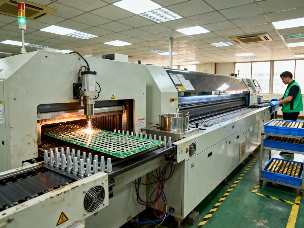
Wave Soldering Process: How It Works, Key Steps, Defects, and PCB Applications

This end-to-end wave soldering guide explains how the process works, from flux application and preheat to wave contact, dwell time, and inspection, then maps every variable to the defects it causes. Packed with profiling techniques, a defect troubleshooting matrix, PCB design rules, procurement checklists, and control plans, it gives manufacturing, engineering, and purchasing teams an honest framework for deciding between conventional wave, selective wave, and reflow in 2026.
PCB Assembly Process Explained: Reflow vs. Wave Soldering and Other Soldering Methods缩略图%
News

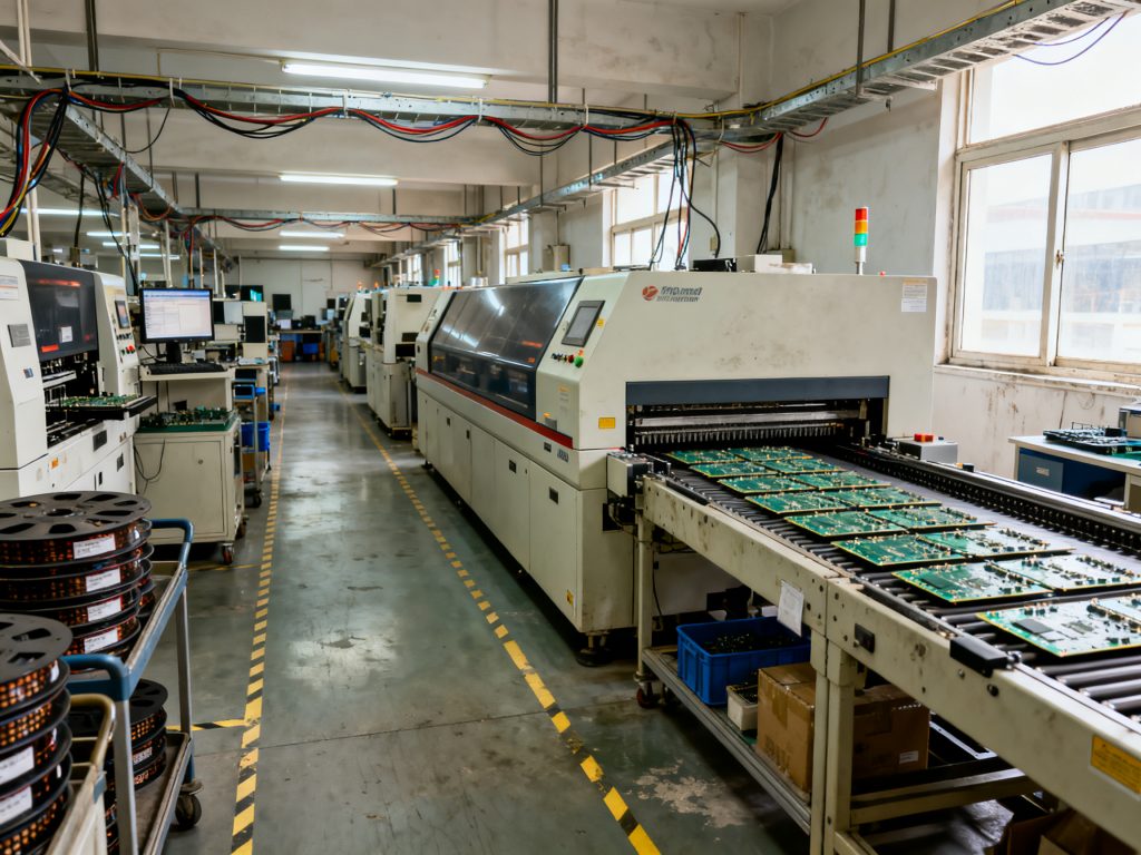
PCB Assembly Process Explained: Reflow vs. Wave Soldering and Other Soldering Methods

PCB assembly is a chain, not a single event, and the soldering method is the biggest lever you control over defect rate, thermal stress, and compliance. This factory-floor guide compares reflow, wave, selective, dip, and manual soldering on process windows, defects, throughput, and cost, then walks through inspection, traceability, and a decision framework for choosing and validating the right method on your own boards before you buy equipment.

Scroll to Top