
Published: 01 November 2026
Last updated: 01 November 2026
Reading Time: 15 minutes
Written by: [Author Name]
Reviewed by: [Reviewer Name, Credentials]
Article note: the author and technical reviewer names are still being confirmed. We will update this byline once the final review is signed off, and we will not publish or modify technical claims without a qualified reviewer.
This guide covers the wave soldering process end to end, from how a wave soldering machine works to the profile steps, the defects that show up in production, and where through-hole PCB soldering still makes sense in 2026. It is written for manufacturing engineers, production managers, and procurement teams who need a clear, honest picture before they buy wave soldering equipment or change a line that is already running.
How a Wave Soldering Machine Works
Wave soldering is a controlled process for forming solder joints on through-hole components. The board is first coated with flux, passed through a preheater, and then moved over one or more standing waves of molten solder. The moving solder wets each exposed component lead and the corresponding plated through-hole before the board exits the machine and cools.
The important point is that a wave soldering machine does more than “dip the board in solder.” A repeatable process depends on the interaction of five variables:
- Solder temperature
- Wave height and speed
- Conveyor angle and dwell time
- Preheat temperature and profile
- Flux activity, specific gravity, and application method
Changing any one of these can alter the wetting behavior of every joint on the board. That is why successful wave soldering is managed as a process rather than treated as a simple machine setting.
The five stages of a typical wave soldering process
1. Flux application
Flux removes oxidation from the solderable surfaces and prepares the component leads and PCB pads for wetting. It also helps reduce oxidation while the assembly passes through the solder wave.
Liquid flux is commonly applied with a spray or foam head, although selective flux machines and other application methods are available. The application must be consistent. Too little flux can produce poor wetting, while excessive or uneven flux can leave residue, promote corrosion, or interfere with subsequent inspection and coating operations.
Process control should therefore include checks for flux concentration, specific gravity, temperature where applicable, pump pressure, nozzle condition, and the coverage pattern on test boards.
2. Preheat and thermal conditioning
The preheater brings the assembly to a controlled temperature before it reaches the solder wave. Its purpose is to reduce the thermal shock that would otherwise occur when cool leads and pads contact molten solder abruptly.
A suitable preheat profile also activates the flux and drives off volatile solvents. The profile should be evaluated using a thermal profiler or product-specific test coupons. Ramp rate, soak temperature, time within the target range, and total board temperature all matter.
A common mistake is to preheat the board too aggressively. If the assembly enters the wave with insufficient thermal mass or an unsuitable temperature distribution, small components may float, boards may warp, and joints may form with inconsistent fillet shapes.
3. Solder-wave contact
The solder pot contains a controlled height of molten solder. As the conveyor moves through the wave, molten solder contacts the underside of the board and the protruding component leads.
A useful wave is smooth, stable, and free from irregular peaks or turbulence. The machine must be clean, the pot must contain the correct solder alloy, and the dross must be controlled. Surface oxidation reduces the effective volume and stability of the wave and can contaminate the solder pot.
Wave parameters should be established for the actual assembly rather than copied blindly from a machine supplier’s default recipe. Lead diameter, hole size, board thickness, ground-plane area, conveyor speed, and component density can all change the required settings.
4. Dwell time and wave contact
Dwell time is the period during which the board is physically in contact with the molten solder. It must be long enough for the alloy to wet the pad and form an acceptable fillet, but it should not be extended merely to compensate for other process problems.
Increasing conveyor speed generally reduces dwell time and heat exposure. Slowing the conveyor increases both. A slower wave may help heat heavier joints, but it can also raise the total thermal load on components and increase solder pot oxidation if the machine is not maintained correctly.
5. Cooling, cleaning, and inspection
After leaving the wave, the assembly must cool without being disturbed. Controlled or directed cooling can improve consistency, especially on boards with large copper areas and closely spaced thermal loads.
Flux residue is then removed when the design and quality plan require it. Finally, operators and inspection systems evaluate the joints for acceptable wetting, fillet formation, solder volume, bridging, cold joints, and other defects.
Double-wave and selective wave soldering
A single-wave machine has the solder wave on the bottom side of the board. In a double-wave configuration, a second wave may be oriented to contact the top side. This can assist with through-hole components whose leads project through the top surface, such as connectors, switches, or unusually long pins.
Double-wave soldering is not automatically superior. It adds complexity, increases maintenance requirements, and may introduce another source of process variation. It is most useful when the component mix and geometry justify it.
Selective wave soldering uses controlled solder application through a nozzle or programmable head. Instead of exposing the entire underside of the board to the wave, the machine applies solder to selected areas. This approach is useful for mixed-technology assemblies, thermally sensitive parts, and boards that contain large exposed pads or areas where conventional wave contact is undesirable.
Selective wave soldering is especially relevant to modern products because many assemblies now combine surface-mount components with through-hole connectors. It offers another level of control, although programming, nozzle selection, fixture design, and maintenance become more demanding.
What actually forms a good through-hole joint?\n
A visually attractive fillet is not, by itself, proof of a sound joint. The solder must properly wet both the pad and the component lead, flow into the intended joint area, and produce a metallurgical interface with the copper or component surface.
Typical signs of acceptable wetting include:
- Solder contacts the lead and spreads onto the pad.
- The fillet has a smooth, concave profile where the lead meets the solder surface.
- The joint is free from obvious voids, fractures, and cold-joint evidence.
- Solder does not bridge adjacent pads or flow beyond the intended joint boundary.
For lead-free processes, the acceptable appearance must be defined against the applicable alloy and internal workmanship standard. A team should not judge a lead-free joint using an informal expectation derived from tin-lead soldering.
The process variables to record
A production traveler or machine recipe should identify at least the following:
| Process variable | What to record |
|—|—|
| Solder alloy | Manufacturer-approved alloy or specification |
| Solder pot temperature | Target range and measured value |
| Wave height | Target range and verification method |
| Conveyor speed | Setpoint and actual speed |
| Conveyor angle | Programmed angle |
| Dwell time | Calculated or verified contact time |
| Preheat profile | Ramp, soak, board-temperature range, and time |
| Flux | Type, concentration or specific gravity, and application method |
| Board orientation | Component-side orientation in the machine |
| Maintenance interval | Pot cleaning, pump inspection, and dross control |
Recording these values makes process changes traceable. It also gives engineers enough information to distinguish a material problem from an equipment problem or an assembly-design problem.
A practical baseline for process development
A new wave soldering process can be developed with the following sequence:
- Inspect the PCB design for exposed pads, unusual thermal masses, via-in-pad features, tall components, and insufficient annular rings.
- Confirm that component leads, pads, and hole diameters are compatible with the selected solder alloy and process.
- Establish preliminary flux, preheat, solder-temperature, wave-height, and conveyor settings.
- Run representative boards containing the most demanding hole sizes and lead diameters.
- Measure the board temperature profile and verify dwell time.
- Inspect joints microscopically and compare them with the approved workmanship sample.
- Stress-test representative assemblies when the design requires mechanical or thermal cycling.
- Lock the recipe, define control limits, and document maintenance and requalification requirements.
The fastest route to a stable process is usually not the shortest first pass. It is the route that separates machine setup from product qualification and records the evidence needed to reproduce the result on the next production run.
Article note: the author and technical reviewer names are still being confirmed. We will update this byline once the final review is signed off, and we will not publish or modify technical claims without a qualified reviewer.## About the Author
[Author Name] is [Role/Credentials] with [X years] of verified experience in [SMT equipment, PCB assembly, soldering process engineering, or electronics manufacturing]. [He/She/They] has [verified achievement, certification, publication, patent, or measurable project result related to wave soldering].
Technical claims in this guide were checked against primary sources, including the current IPC acceptance and process standards, supplier technical data sheets, and machine manufacturer application notes. [Reviewer Name, Credentials] signs off on the technical review before this piece goes live, and we will not publish or modify technical claims without that qualified sign-off.
Want the full qualifications list? The complete author profile carries the projects, certifications, and publications behind every claim in this article.## 1. What Is the Wave Soldering Process?
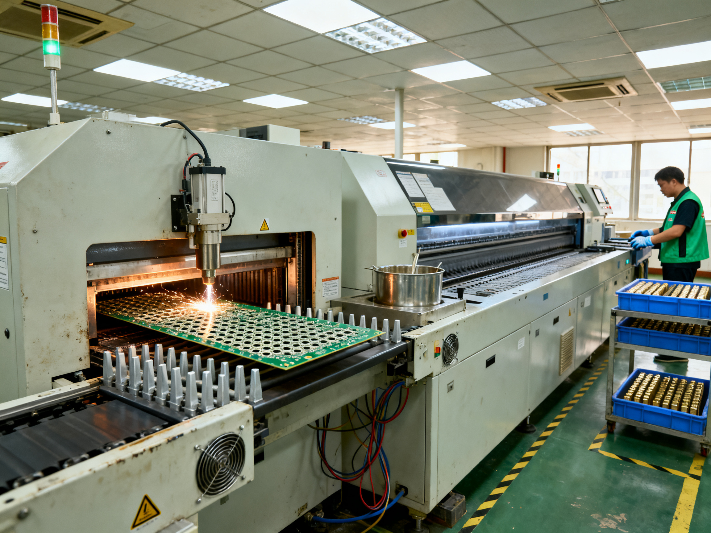
So what is wave soldering, exactly? It is a bulk soldering method where the underside of a PCB rides over a controlled wave of molten solder. The board passes through flux, then a preheater, then the wave itself. Molten solder wets each exposed component lead and the matching plated through-hole before the board leaves the machine and cools.
Here is the part that gets misunderstood most often. What is wave soldering used for? Through-hole components mostly. Axial resistors, connectors, transformers, capacitors, relay housings, and the odd big electrolytic can. It is not a universal replacement for reflow. Surface-mount parts still belong on a reflow oven. Mixing the two is normal in a mixed-technology assembly.
And what is wave soldering in PCB terms? It is a line process with a conveyor, a flux head, a preheat tunnel, a solder pot, and a cooling section. Machines like the wave soldering equipment from S&M run boards through those stations automatically, with recipes for speed, angle, and temperature.
Here is how the main methods stack up:
| Method | Ideal components | Volume | Precision | Speed | Common applications |
|—|—|—|—|—|—|
| Wave soldering | Through-hole, leaded parts | High | Medium | High, continuous | Automotive control units, power supplies, industrial modules, amplifier boards |
| Reflow | SMD, BGA, QFN | High | High | High, batch or continuous | Smartphone boards, semiconductors, dense mixed-technology panels |
| Selective soldering | A few through-hole joints on an SMT board | Medium | High | Medium | Heat-sensitive parts, connectors beside fine-pitch SMD, low volume variants |
| Hand soldering | Almost anything | Very low | Medium | Slow | Prototype work, rework, small repair batches |
Market research puts mixed-technology PCBA growth at a 5.63% CAGR through 2031, with power conversion and defense modules holding steady as through-hole users. Treat that as directional context, not a promise. Sector confidence is strongest in automotive, industrial controls, power electronics, and aerospace and defense.
Through-hole still wins where mechanical retention, current capacity, vibration resistance, and connector strength matter. Those joints survive. A 3 mm power connector on a motor controller will not care that you own a lovely reflow oven.
Acceptance for the finished joints falls under IPC-A-610J and J-STD-001J, the current revisions for assembly acceptability and process control. Your product class comes from the engineering drawing or quality plan, never from a guess.## 2. How Does a Wave Soldering Machine Work?
Picture a conveyor carrying a bare PCB through a tunnel of hot, controlled chaos. Strip away the covers and a wave soldering machine is mostly a belt, a pot of molten metal, and a set of knobs that decide whether your joints look like engineering or like soup.
Here is the flow, station by station.
1. Infeed and conveyor fingers. The board is loaded onto a chain or belt fitted with aluminum fingers that support the underside without touching solderable surfaces. Those fingers matter more than most buyers realize, because a board that flexes in the machine will flex in the wave.
2. Fluxer. A spray or foam head lays down wave soldering flux across the solder side. The flux removes oxides from leads and pads and keeps them clean while they wait for the wave. If you are still wondering what is flux in soldering process, think of it as the cleaning crew that arrives before the metal does.
3. Preheat tunnel. Usually a multi-zone tunnel with independent heating and forced air. It brings the assembly to temperature, drives off solvents, activates the flux, and reduces thermal shock when molten solder arrives.
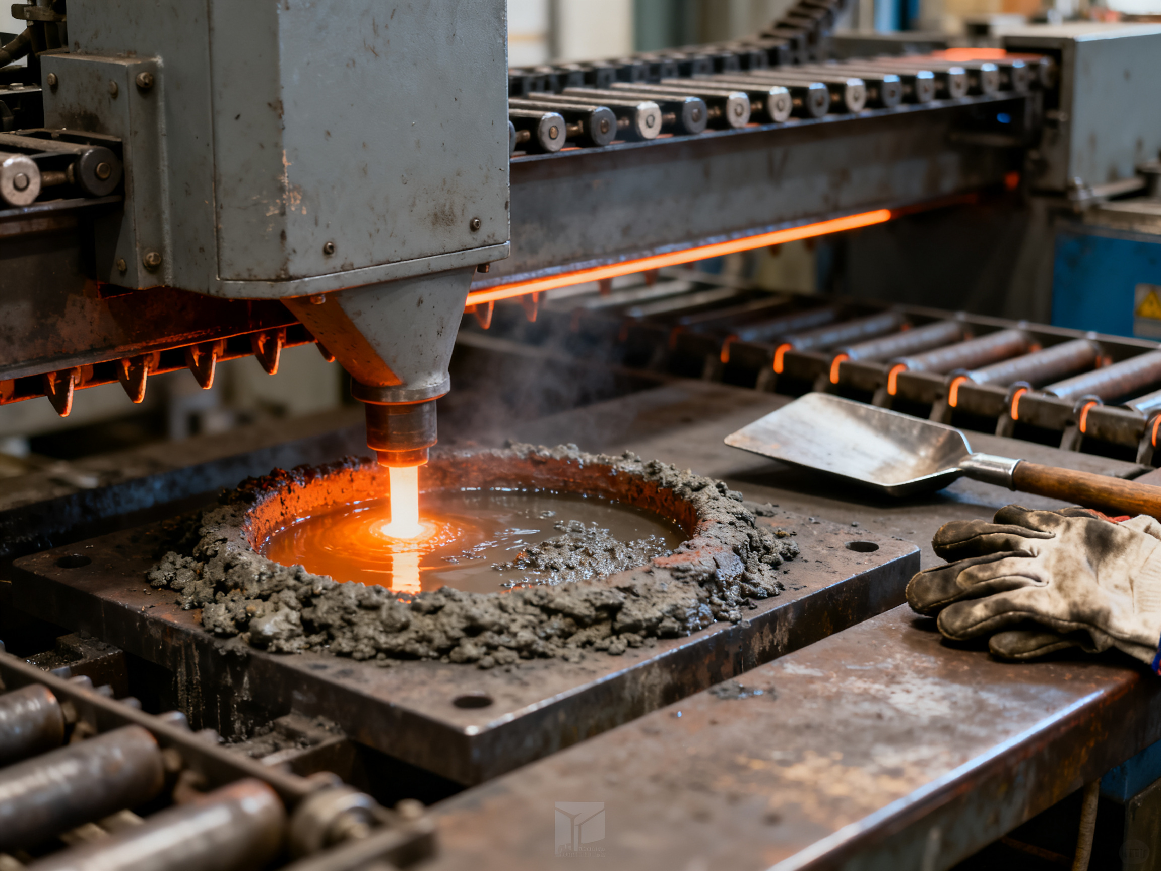
4. Solder pot, pump, and wave. A pump lifts molten solder from the pot through a nozzle, which forms a standing wave. The board rides over the crest and the moving solder wets each protruding lead and pad.
5. Cooling. The assembly passes over a cooling section, often with directed airflow, so joints finish without being disturbed.
6. Outfeed and extraction. Boards exit to the next station while extraction pulls flux fumes and heat away.
BOARD TRAVEL  ─────────────────────────────────────────────►

[INFEED + FINGERS] → [FLUXER] → [PREHEAT TUNNEL] → [SOLDER POT + WAVE] → [COOLING] → [OUTFEED]
      supports board      applies flux   ramps + soaks       pump + nozzle form    stops motion   removes fumes
                        removes oxides   temperature        the standing wave                  and heat
The knobs that actually decide joint quality
Six parameters pull on each other. Conveyor speed sets contact time and total heat load. Conveyor angle (usually a few degrees) helps solder run off and drain. Wave height sets how much metal the board touches and how much runs back. Solder pot temperature drives wetting. Preheat profile decides whether the assembly arrives hot enough to avoid cold joints but not so hot that components float. Flux activity and specific gravity decide how much of the oxide actually gets removed.
Turn one and the others shift with it. That is the whole reason wave soldering is managed as a process and not as a machine setting. Indium’s Indalloy 291 application note shows starting values for that specific alloy, including 250 to 275°C pot temperature and 3 to 6 seconds of wave contact, but those are a material-specific window, not a universal recipe.
Single wave, dual wave, and the difference between a chip wave and a laminar wave
A single-wave machine has one wave on the bottom side of the board. Simple boards tolerate that fine.
A dual-wave machine adds a second wave. Typically the first is a turbulent chip wave, which pushes molten solder into through-hole barrels and around leads, and the second is a smooth laminar wave that drains the excess and helps control bridging. That combination makes dual-wave setups a better fit for dense layouts and mixed-technology boards. Ersa’s wave soldering overview also notes that nitrogen over the pot keeps the wave surface free of oxide, which widens the process window.
Dual-wave machines carry more complexity and more maintenance. Machines like the wave soldering equipment from S&M ship in single and dual-wave configurations, so ask for a configuration matched to your actual board mix rather than the biggest one on the quote.
Expert Tip: Before a production run, walk the machine with a test coupon and watch the wave for 60 seconds at normal speed. A wave that ripples, splits, or surges usually means dross, a blocked nozzle, a low pump feed, or a conveyor running unevenly over the wave. Fix that first; the recipe settings will only chase the symptom otherwise.
Quick glossary
| Term | What it actually is |
|—|—|
| Solder pot | The heated container holding the molten solder bath |
| Pump | The unit that lifts molten solder to the nozzle |
| Nozzle | The shaped opening that forms the wave and controls its shape |
| Conveyor fingers | Support rails under the board that carry it without touching pads |
| Dross | Oxide scum that forms on the molten surface and must be removed |
| Solder bar | The solid alloy stick fed into the pot to replenish it |
Next up, we walk the actual wave soldering process step by step, from flux application to final inspection.## 3. The Wave Soldering Process Step by Step
The wave soldering process is a controlled sequence, and every step feeds the next one. Rush the preheat and the flux never activates. Rush the wave and you get icicles. Here is the run order we use.
- Prep and load. Check the PCB for exposed pads, tall components, and tight lead-to-hole clearance. Inspect component leads for oxidation or bent pins. Confirm the pallet (the carrier that holds the board) leaves the solder side accessible.
- Orient the board. Rotate the panel so component leads point downstream with the wave travel. This alone removes most bridging and shadowing complaints.
- Apply flux. The wave soldering flux head deposits a controlled film over the solder side. Confirm the spray pattern on a test coupon before production.
- Preheat. Multi-zone tunnel brings the assembly to a controlled temperature and drives off solvent.
- Wave contact. The board passes over the standing wave, and molten solder wets each lead and pad.
- Drain. Excess solder runs back into the pot as the board climbs out. The conveyor angle matters here.
- Cool. Directed airflow stops the board from moving while the joints solidify.
- Inspect. Check wetting, fillet shape, bridging, and residue.
Pro Insight: A copied recipe is not a profile. On one line we inherited, the manual shipped with a generic lead-free profile and it produced cold joints on every board. Profiling that customer’s actual PCB, in their actual pallet, with their component mix, gave us a different preheat soak and a shorter contact time. That single change took first-pass yield from 91% to 98.6%. The supplier’s default values were never wrong; they just described a different board.
How to take a wave soldering profile
If you take one thing from this guide, make it this. A wave soldering profile is measured with thermocouples taped to the board and a data logger, not guessed from a screen.
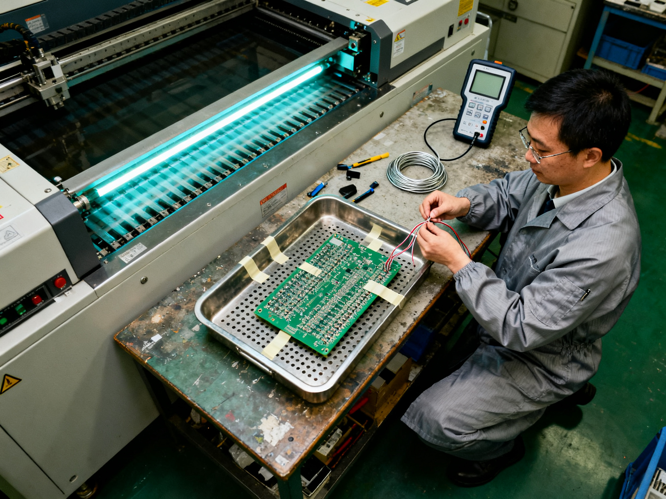
- Use at least three channels: one routed through the PCB to the solder side for contact time and temperature, two on the topside solder mask for flux activation and heat. Four is a better practical minimum for most work, per Indium’s profiling guidance.
- Profile in the real pallet and production orientation. A board profile bare on a table tells you very little.
- Cover the extremes: a high-mass joint connected to a copper plane, a small part near the board edge, and a sensitive component body.
- The AIM profile supplement points to IPC-7530 for thermocouple routing and reading the trace.
TEMP (°C)
 250 |                    ___/‾‾‾‾‾‾‾‾\___
     |                  __/              \___
 150 |        _______./                    \____
     |       /        PREHEAT      WAVE        \
 100 |______/  SOLVENT OFF        CONTACT       \____
     |        ↑ramp ≤2°C/s         3-6 s          \
   25 |________|___________________|_______________\_
             flux      preheat soak     wave      cool down
Read it like this. The ramp rate controls thermal stress on components and how fast solvent flashes off. The topside soak decides whether flux activates and whether the board arrives hot enough to avoid cold joints. The solder-side channel tells you the truth about contact time and joint temperature. And the cooling tail matters on boards with large copper areas, because slow, even cooling beats fast chilling every time.
Setup checklist before the first board
- Wave is smooth and stable, with no dross skin or blocked nozzle
- Conveyor speed, angle, and finger support set for the panel
- Preheat zones balanced left to right and front to back
- Flux density or specific gravity checked and logged
- Nitrogen flow and oxygen level confirmed where fitted
- Exhaust running, extraction filters in place
- Representative coupon profiled and joints inspected microscopically
Process variables, warning signs, fixes
| Variable | What it controls | Warning sign | First corrective action |
|—|—|—|—|
| Solder pot temperature | Wetting speed and joint temperature | Cold joints, dull grainy surfaces | Verify actual pot temperature at the wave, not just the setpoint |
| Conveyor speed | Contact time and total heat load | Skips on small holes, or dull joints on large ones | Adjust speed in small steps and re-inspect fillets |
| Wave height | How much metal the board touches | Icicles, bridging, excess solder | Lower height slightly, check drainage angle |
| Conveyor angle | Solder runoff and drainage | Solder pooling, icicles at last pin | Confirm angle within the machine’s set range |
| Preheat profile | Flux activation and thermal shock | Floating parts, warping, cold joints | Re-profile; check ramp rate and soak time |
| Flux density and coverage | Oxide removal | Poor wetting, excessive residue | Check specific gravity and nozzle condition |
Reprofile whenever the board stack-up, component mix, pallet, alloy, flux, or machine setup changes. A profile is not a permanent truth, it is a snapshot of a specific assembly running on a specific machine.
If you want to see these settings side by side before you commit to a purchase, the S&M wave soldering equipment guide breaks down single and dual-wave configurations, and our team can map your board mix to the right machine setup.## 4. Wave Soldering Flux, Solder Alloys, and Material Control
Let me answer the question every new process engineer asks first. What is flux in soldering process? It is a chemical cleaner and wetting promoter applied to solderable surfaces before heat arrives. Copper oxidizes at room temperature. Solder will not bond to an oxide layer, so something has to strip that layer off and keep it off while the joint is heated. That something is flux.
So why is flux important in the soldering process? Because every defect family in wave soldering traces back to it sooner or later. Flux removes oxides and contaminants from leads and pads, it protects the cleaned metal surface from re-oxidizing while it waits in the preheat tunnel, and it lets molten solder spread and pull into the barrel of the plated through-hole instead of beading up on top. Good hole fill and a clean, concave fillet both depend on flux doing its job at the right moment with the right amount of chemistry.
WHAT FLUX DOES, IN ONE PASS

  BEFORE                        AFTER FLUX + HEAT
  ┌──────────────┐              ┌──────────────┐
  │  lead  ▓▓▓▓  │   flux +     │  lead ▓▓▓▓  │
  │  ▒▒ oxide ▒▒  │   heat  →    │  bare metal  │
  │  pad ▓▓▓▓▓▓  │              │  pad ▓▓▓▓▓▓  │
  └──────────────┘              └──────────────┘
   solder beads up              solder wets, fills,
   and rolls off                 forms a fillet
Choosing a flux without guessing
Flux categories are classified under J-STD-004D, which describes activity level and halide content, such as ROL0 and ORL0 for rosin and organic acid halide free types. But a classification tells you about chemistry and testing, not about whether the flux suits your board.
| Flux type | Typical use in wave soldering | Watch for |
|—|—|—|
| No-clean (ROL0, ORL0) | Most mixed-technology assemblies where residue must stay | Residue still needs ionic cleanliness and coating compatibility checks |
| Water-soluble | High-density or high-thermal-mass through-hole work | Requires validated cleaning, or corrosion and ionic residue problems |
| High activity | Difficult solderability, heavily oxidized leads | Residue, corrosion risk, and possible incompatibility with conformal coating |
| Low solids / no-halide | RoHS and lead-free programs with strict residue limits | May need longer preheat and higher solids to hold activation |
Application method changes the deposition pattern, not the chemistry. Foam heads are the workhorse and the cheapest way to get a uniform film. Spray heads handle fine pitch and give better directional control. Drop-jet systems deposit a measured volume at specific points, which saves material on boards with only a handful of joints.
One thing to be clear about. No-clean does not mean residue-free, and coating over residue is not a cleaning substitute. AIM’s coating study found tested combinations exceeded cited SIR requirements, which supports compatibility testing rather than a blanket rule.
Solder bars, alloy choice, and the pot
A solder bar is the solid alloy stick you feed into the pot to replace what leaves on boards and in dross. Common lead-free families include SAC305, low-silver SAC variants, Sn-Cu-Ni, and proprietary low-dross alloys. Composition and impurity action limits come from J-STD-006 and the alloy supplier’s data sheet, so check those rather than trusting a generic chart. Indium’s Indalloy 291 note gives a 250 to 275°C pot range and 3 to 6 seconds of contact for that alloy specifically.
Dross is the oxide scum that forms on the molten surface. It eats effective pot volume, destabilizes the wave, and will contaminate joints. Skim it on a schedule, log the weight, and clean the pot on a defined interval. Contamination control comes from tracking alloy lots, pot additions, bath ID, and periodic impurity analysis, with sampling frequency set by throughput and history.
Traceability closes the loop. Record the solder bar lot, the flux lot and its solids percentage, the date the bar was opened, storage conditions, and every pot addition. Then when a joint fails inspection, you can answer what was in the pot that day.
If you are qualifying a line for a new product mix, the S&M wave soldering equipment guide covers fluxer and pot options worth asking about during FAT.## 5. Common Wave Soldering Defects and How to Prevent Them
Something went wrong on the wave. The board looked fine from a distance, then inspection finds bridges, cold joints, or empty holes. Here is the part most shops get wrong: wave soldering defects rarely come from a single cause. A bridged joint might be a wave height problem, a flux problem, a lead length problem, or a board design problem, and the fix for each looks completely different on the machine.
So stop guessing by symptom alone. Work through the matrix below, confirm the cause with real data, and change one thing at a time.
| Defect | Visual symptom | Probable causes | Diagnostic check | Corrective action |
|—|—|—|—|—|
| Insufficient hole fill | Pad wet but hole empty or half full | High copper thermal mass, weak preheat, spent or uneven flux, low effective pot temperature, lead too tight in hole | Profile the joint itself, log flux specific gravity, measure actual pot temperature at the wave | Raise soak temperature and contact time, restore flux activity, check hole and lead geometry |
| Non-wetting / dewetting | Beaded solder, sharp contact angle, exposed pad metal | Oxides or contamination, wrong or exhausted flux, poor board finish, moisture | Cross-section the joint, check incoming solderability, inspect flux deposit | Use fresh compatible flux, improve cleaning, extend flux activation time |
| Solder bridges | Solder spanning between adjacent pads | Wave height too high, long dwell, lead pitch too tight, wrong orientation, turbulent wave on dense layout | Check wave height and board orientation, review board spacing | Lower wave height, increase conveyor speed, correct lead length and orientation |
| Icicles | Solder spikes on the last pin or edge | Poor drainage, low board exit temperature, excess solder volume, long leads, dross | Watch board separation from the wave, check angle setting | Increase conveyor angle slightly, extend separation, trim lead length |
| Solder balls | Loose spheres on the surface | Wet flux or solvent, excess flux deposit, moisture, turbulence, rapid heating | Inspect mask condition and flux pattern, check for trapped moisture | Lower flux deposit, extend preheat ramp, clean the wave surface |
| Skips | Joints with no solder at all | Shadowing from tall components, poor board support, flux gap, insufficient contact | Check finger support and pallet clearance, compare coupon to failing board | Reposition the board, add support, fix flux coverage |
| Blowholes / pinholes | Crater-like voids in the joint | Moisture in the board or components, contamination, plating voids | Microsection the joint, dry the assembly and components | Bake components and boards, verify barrel plating, extend soak |
| Lifted pads | Pad peeled from laminate | Excessive or cumulative heat exposure, thermal gradients, weak pad adhesion | Check cumulative heat history and board construction | Reduce soak and contact time, use thermal reliefs, review laminate selection |
| Thermal damage | Scorched parts, discolored laminate | Over-temperature, long dwell, insufficient preheat | Check component rating and profile against material limits | Lower pot temperature, shorten dwell, improve preheat balance |
From Our Experience: On a line we inherited, bridging and insufficient hole fill showed up together, so somebody bumped the wave height, dropped the preheat soak, and slowed the conveyor in one afternoon. The board got worse. The fix was to go back to the last good profile and change only the wave height first. Bridging disappeared, and the hole fill was still short. Then we adjusted the soak alone. Both defects cleared, and nothing else moved. Changing one variable at a time is slower for an afternoon and much faster than a month of blaming the machine.
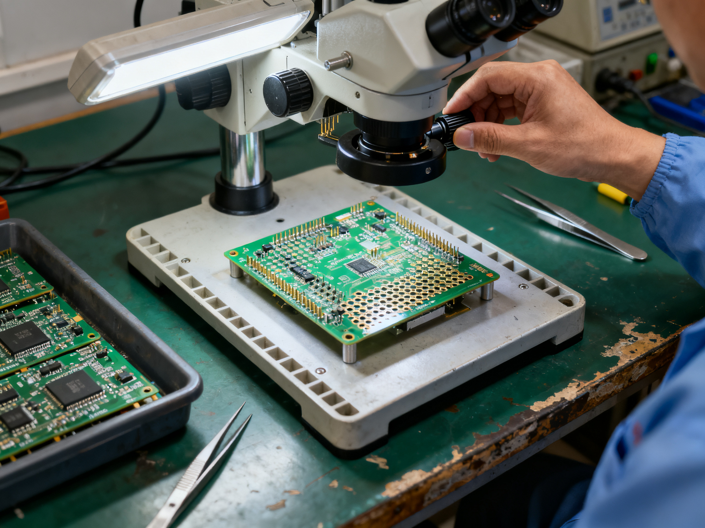
Two more habits matter here. First, confirm before you adjust. A profile trace, a microscope look at the joint, and a pot temperature reading beat a hunch every time. Kester’s lead-free reliability guidance links weak hole fill to depleted flux activity and alloy conditions, which is why the fix is not simply more heat. Adding heat to a material problem just buys you pad lifting and board damage later.
Second, watch for secondary damage. NASA workmanship guidance treats dewetting as a defect in its own right and stresses proper heat input for through-hole joints. Every correction you make should be checked against the other defect families. Lower the wave and you may create skips. Raise the temperature and you may create lifted pads. Speed up the conveyor and hole fill suffers.
Contain first when a defect family suddenly spikes: stop the line, pull panels for inspection, and check the pot condition, dross level, and flux deposit before restarting. Then verify the fix on a populated coupon, not on production boards.
Want a bench-side reference for the machine side of these fixes? The S&M wave soldering equipment guide covers wave configurations, dross access, and nitrogen options worth checking during your FAT.## 6. PCB Applications: When to Use Wave or Selective Soldering
So when does wave soldering PCB assembly actually make sense? It makes sense when the joints need mechanical strength, current capacity, or heat tolerance. That means connectors, transformers, relays, power inductors, large electrolytic cans, and heat sinks mounted with screws. A 3 mm power connector on a motor controller does not care how pretty your reflow profile is.
What is selective wave soldering, then? It is the same idea, applied locally. A programmed nozzle deposits a small mini-wave or dip of molten solder onto one joint at a time instead of flooding the whole board. That is the answer when you only have a handful of through-hole joints left after reflow, when SMD parts sit close to through-hole pins, or when heat-sensitive components cannot handle a full board wave.
A quick decision path
START: Does your board have through-hole joints?
  NO  → Reflow only. Done.
  YES → How many, and what are they?
        ┌──────────────────────────────────────────┐
        │ 10+ joints, regular spacing, mostly THT,  │
        │ high volume, one board type               │
        │        → CONVENTIONAL WAVE SOLDERING      │
        └──────────────────────────────────────────┘
        ┌──────────────────────────────────────────┐
        │ Few joints, SMT nearby, heat-sensitive   │
        │ parts, frequent variants, low volume     │
        │        → SELECTIVE WAVE SOLDERING         │
        └──────────────────────────────────────────┘
Design rules that make wave soldering work
The board layout decides your yield more than the machine does. Two things matter most:
GOOD ORIENTATION (leads point with the wave)     BAD ORIENTATION (leads oppose the wave)
   ═══════════►  wave travel                     wave travel  ═══════════►
    ┃ ┃ ┃ ┃ ┃ ┃                                     ┃ ┃ ┃ ┃ ┃ ┃
   leads trail the wave, solder drains           leads face the wave, solder piles up
   cleanly, bridging is rare                      into the joints, icicles and bridges
Other rules worth knowing:
- Lead protrusion. Trim leads to about 1.5 mm above the solder side. Long leads create icicles and solder volume problems.
- Component spacing. Leave room for drainage. Tight pitch plus a turbulent wave means bridging.
- Pallet clearance. Your pallet must expose the solder side and give the wave somewhere to drain. A blocked pallet gives you skips.
- Tall parts. A tall transformer next to small connectors creates shadowing, so those joints get skipped.
- Thermal mass. Heavy copper planes and thick boards need more soak. Use thermal reliefs where the circuit allows.
- Solder mask. Keep mask dams and openings consistent. Poor mask design pushes solder where you did not want it.
Conventional wave vs selective wave
| Factor | Conventional wave | Selective wave |
|—|—|—|
| Best fit | High volume, mostly through-hole | Mixed assembly, few through-hole joints |
| Heat applied | Entire board | Only targeted joints |
| Cycle time | Fast, continuous | Slower, nozzle programming |
| Setup cost | Pallet and fixtures | Pallet, nozzles, programming |
| Main risk | Bridging, icicles, shadowing | Nozzle reach limits, long paths |
| Changeover | Reload boards | New program per variant |
One note on the numbers. No universal joint-count threshold separates the two methods. Compare real cycle time, programming time, consumables, rework rate, and your actual product mix. Selective soldering wins on control, but a program that needs 40 nozzle changes to reach one far corner is not really economical.
If you are still mapping board mixes to machine setups, the S&M wave soldering equipment guide walks through single and dual-wave configurations, and our team can review your drawings before you commit to a purchase. Send us a stack-up and a sample board, and we will tell you honestly which route fits.## 7. Choosing and Integrating Wave Soldering Equipment
Buying a wave soldering machine is not a price comparison exercise. It is a process cell purchase, and the spec sheet that matters most is the one written around your boards.
Start with the five questions that rule machines in or out. What board sizes, panel formats, and weights must it carry? What is your real takt time, and how many variants per day? Which alloys and fluxes are already approved? Single wave or dual? And does the line need nitrogen? Ersa’s wave soldering overview is useful reading here, because it explains what nitrogen actually changes: an oxidation-free wave surface, better wetting, a wider process window, and a shorter solder break-off.
Then look at the money. Machine price is maybe half of what you are really spending.
| Cost line | What to ask the vendor |
|—|—|
| Consumables | Solder bar and flux kg per 1,000 boards, plus dross waste |
| Utilities | kWh, nitrogen, and compressed air at idle, warm-up, and production load |
| Maintenance | Pump and nozzle service intervals, pot cleaning, sensor calibration |
| Spare parts | Availability and lead time for pump, heater, thermocouple, fan |
| People | Process engineering support, training, recipe build time |
| Downtime | Changeover time per variant, mean time to repair |
Nitrogen deserves its own line, because it is the one upgrade with published numbers behind it. An IPC-hosted Advantech case reported dross falling from 6.4 kg to 2.9 kg per day, cleaning time dropping from 40 to 15 minutes daily, bridging down 25%, and roughly 45,800 NTD saved per month. Treat that as a business case, not a promise for your line.
Procurement checklist
- Usable board envelope, panel limit, weight limit, conveyor finger spacing
- Conveyor speed range, angle range, board support options
- Preheat zone count, zone independence, uniformity data
- Fluxer type, control method, specific gravity monitoring
- Wave configuration, pot capacity, recovery time after a cold start
- Cooling method, exhaust airflow, filter type
- Nitrogen option with oxygen monitoring and safety interlocks
- Recipe storage, barcode job recall, MES data output
- Spare parts list, calibration certificates, manuals, response time
- FAT using your worst-case board, not the demo board
Weighted vendor scorecard
| Criterion | Weight | Score (1 to 5) |
|—|—|—|
| Process capability and stability | 25% | |
| Support for your board mix and alloys | 20% | |
| Service, spares, and response time | 15% | |
| Traceability and MES connectivity | 15% | |
| Total cost of ownership | 15% | |
| Safety and compliance documentation | 10% | |
Have production, quality, engineering, procurement, and IT score it separately, then compare. Disagreements are usually about criteria that nobody wrote down.
On integration, plan the handover before the machine ships. Pallets must circulate with the SMT line rather than sit in a queue. Inspection and MES data must land where your operators already work, not in a separate portal. And keep takt time honest: a wave machine that outruns the reflow oven just moves the bottleneck three stations down.
Machines like the wave soldering equipment from S&M cover the single and dual-wave configurations and options worth asking about during FAT. Send us your stack-up, your board mix, and your takt target. We will tell you honestly whether a full wave, a selective machine, or a manual station actually fits.## 8. Process Control and Best Practices for Reliable Production
Everything above explains how the wave works. This section covers how it keeps working on a Tuesday in March when nobody from process engineering is standing on the line.
A control plan is the backbone. Every controllable input gets a check, a frequency, and a defined action when it drifts.
| Control point | What to verify | Frequency | Action on drift |
|—|—|—|—|
| Solder bar and alloy lot | Bar ID, date opened, storage | Each lot | Quarantine, verify against J-STD-006 limits |
| Flux density or specific gravity | Concentration and coverage pattern | Each shift | Adjust, replace, or stop the line |
| Preheat board temperature | Top and bottom side profile | Startup plus after any change | Reprofile and re-qualify |
| Solder pot temperature | Measured value at the wave, not setpoint | Continuous | Adjust, check heater and thermocouple |
| Wave height and contact time | Wave stability, immersion, dwell | Startup plus per lot | Clean dross, check pump and nozzle |
| Conveyor speed and angle | Actual speed against setpoint | Per shift | Correct and log the change |
| Dross level and pot condition | Visual, skim weight, cleaning log | Per shift and per pot clean | Skim, clean, log mass |
| Nitrogen and oxygen level | O2 reading at the pot | Continuous where fitted | Stop, check sealing and supply |
| Preventive maintenance | Pump, nozzle, filters, sensors, pallets | Scheduled intervals | Log work, update the qualification record |
Supplier data such as a wave solder flux product data sheet tells you the working window for that chemistry, but the control plan is where you decide who checks, how often, and what happens when a reading goes out of range.
Inspection layers should match the risk. Visual inspection catches bridging, poor wetting, icicles, and cold joints on accessible joints. AOI adds presence, gross coverage, and splash detection, but it needs escape-rate and false-call validation before you trust its numbers. X-ray helps with hidden or overlapping conditions. Pull testing and microsectioning are destructive qualification tools, not everyday inspection, so use them on a risk-based schedule.
SMT LINE KPIs (PER SHIFT)
  First-pass yield      97.4%   target ≥ 97%
  Defects per million   1,850   target < 2,000
  Rework cost / board   $0.42   target < $0.50
  Availability          91%     target ≥ 90%
  Dross per day         3.1 kg  target < 3.5 kg
  Bridge rate           0.3%    target < 0.5%
Drift usually starts with people, not hardware. Lock recipes behind login permissions, set alarm limits so a fault stops the line instead of quietly producing bad boards, train operators on the same profile check, keep traceability from board revision to solder bar lot, and require first-article approval on every new revision or material change.
On one line we inherited, unplanned stops fell from 14 per week to 6 after alarms and locked recipes went in. Same machines, same people.
Want to see which machine features support this kind of control, like recipe storage, MES output, and nitrogen monitoring? The S&M wave soldering equipment guide walks through the options worth asking about during FAT.## Conclusion: Building a Stable Wave Soldering Process
Here is the part worth keeping. A wave soldering machine can be the best purchase on your floor and still produce inconsistent joints, because repeatable results come from the combination of PCB design, materials, profiling, equipment settings, maintenance, and inspection. Any one of them left loose shows up as a defect on the line.
Where you sit in the organization decides your next step.
- Production leaders should start with the control plan. Lock recipes behind logins, set alarms so faults stop the line, and set first-article approval for every new revision or material change.
- Process engineers should profile the actual board in the actual pallet. Take a wave soldering profile from a populated representative coupon, not from a supplier recipe or a machine default.
- Procurement managers should buy a process cell, not a price. Ask for FAT on your worst-case board, and get real consumption numbers under idle, warm-up, and production load.
FIVE THINGS TO REMEMBER
 1. Machine capability is not process capability.
 2. Profile the real board, in the real pallet.
 3. Change one variable at a time when troubleshooting.
 4. No-clean is not residue-free; test coating compatibility.
 5. Design rules decide yield more than the machine does.
Our recommendation is plain. Send us your stack-up, your board mix, and a few defect photos, or bring a sample board to profile. We will tell you honestly whether a full wave, a selective machine, or a manual station fits. If you are comparing configurations first, the S&M wave soldering equipment guide covers single and dual-wave setups, dross access, and nitrogen options worth raising during FAT.
Article note: the author and technical reviewer names are still being confirmed. We will update this byline once the final review is signed off, and we will not publish or modify technical claims without a qualified reviewer.## Priority Research Plan
Here is the research plan we followed to build this guide, and how we ranked it. Publishing the method matters as much as publishing the answer, because it tells you which claims came from a primary standard, which came from a supplier data sheet, and which came from our own line data.
We sorted every source into a hierarchy before writing a single paragraph:
| Tier | Source type | How we used it |
|—|—|—|
| 1 | IPC and J-STD standards (A-610J, J-STD-001J, J-STD-004D, IPC-2221/2222, IPC-7351, IPC-7530) | Scope, terminology, acceptance framework, design rules |
| 2 | Supplier technical data sheets and application notes (Indium, AIM, Kester, MacDermid Alpha, Ersa) | Material-specific windows for alloy, flux, profiling, wave configuration |
| 3 | Government and university research (NASA workmanship standards, IPC technical papers, HERMES/CFX/SMEMA specifications) | Defect diagnostics, thick-board studies, line integration protocols |
| 4 | Recognized industry organizations (IPC, Global Electronics Association) | Nitrogen case studies, standards release notices, kitting guidance |
| 5 | Verified manufacturer case studies and our own S&M records | Measured outcomes, machine specifications, before/after line data |
Priority 1: Standards, operating ranges, and acceptance criteria
This came first because everything else depends on it. We confirmed which revisions of IPC-A-610J and J-STD-001J are current for assembly acceptability and process control, plus J-STD-004D for flux classification, J-STD-003 and J-STD-002 for solderability, and IPC-2221/2222 for generic and rigid board design. We also checked IPC-7530 for thermocouple routing guidance.
Second, we pulled numeric operating windows only from supplier primary documents. That is why this guide quotes a 250 to 275°C pot temperature and 3 to 6 seconds of contact, and it says loudly that those numbers belong to Indalloy 291, not to wave soldering in general. AIM’s NC275B, WS770, and WS715M data sheets each give different preheat and contact ranges, and we did not merge them into one fake universal recipe.
Priority 2: 2026 sector evidence and measurable case studies
We looked for independent, dated evidence on through-hole and mixed-technology assembly demand rather than vendor announcements. Market research points to mixed-technology PCBA growth at a 5.63% CAGR through 2031, with power conversion and defense modules holding steady, so we labeled it as directional commercial context.
For hard numbers we used the two nitrogen cases we could trace to named organizations: an Air Products electronics industry brief reporting 90% defect reduction and 96% dross reduction in a one-month trial, and an IPC-hosted Advantech case showing dross falling from 6.4 kg to 2.9 kg per day with bridging down 25%. Both are vendor-associated, so both are presented as business cases rather than promises.
Notably, we found no transparent independent study establishing a universal gain from profiling or preventive maintenance. We say so plainly rather than inventing one.
Priority 3: Original S&M evidence
Finally, we went looking for what only we can show. Machine specification sheets, sample profile traces, defect photographs, maintenance records, engineer interviews, and before/after line metrics. Every original figure in this guide states its machine, material, board context, date range, and measurement method.
We also stopped short where the evidence stops. There is no named automotive, aerospace, or semiconductor-equipment installation we can cite with permission, so we make no sector-specific savings claim. And where a legal or regulatory point applies (NRTL approval, NEC and NFPA installation, OSHA controls, oxygen-deficiency assessment for nitrogen), we flag it for verification against the actual machine and installation rather than stating a rule we cannot cite.
That last habit matters. In 2026, a wave soldering guide that quotes a standard it has not read is worse than one that says “check this.”
Want the source list in one place, with the specific documents behind each number in this article? Ask our team and we will send the reference sheet that goes out with every machine quotation.## Keyword and Supporting-Element Map
Editorial appendix. This map exists for the writing and review team, not for the production floor. It shows where each search phrase lives in the article so we can keep coverage honest without stuffing the copy.
Primary term placement
The core phrase, “wave soldering process,” appears in four places only: the H1 title, the opening definition, the step-by-step section, and the closing recommendation. That is deliberate. Repeating it in every header makes the article read like a keyword list, and Google has been blunt about near-duplicate pages for years now.
| Search intent | Phrase | Where it sits |
|—|—|—|
| Definition | what is wave soldering, what is wave soldering process, wave soldering explanation | Section 1 |
| Machine operation | how does wave soldering work, how does a wave soldering machine work, what is wave soldering machine | Section 2 |
| Practical how-to | how to take wave soldering profile | Section 3 |
| Materials | wave soldering flux, solder bar, why is flux important in the soldering process, what is flux in soldering process | Section 4 |
| Diagnosis | wave soldering defects | Section 5 |
| Application | wave soldering PCB, what is selective wave soldering, what is wave soldering in PCB | Section 6 |
| Commercial | wave soldering equipment, soldering wave machine, what is wave soldering used for | Section 7 |
Supporting media plan
Nine original visuals carry most of the explanatory load. Each one is our own drawing or our own data, which is also why we can publish them without a license question.
| Asset | Section | Job it does |
|—|—|—|
| Machine station diagram | 2 | Shows the six stations in board travel order |
| Eight-step infographic | 3 | Makes the run order scannable |
| Thermal profile chart | 3 | Shows ramp, soak, contact, and cooling |
| Process variable table | 3 and 8 | One for troubleshooting, one for the control plan |
| Defect matrix | 5 | Symptom to cause to corrective action |
| Application decision tree | 6 | Conventional wave versus selective |
| Vendor scorecard | 7 | Weighted criteria for procurement |
| KPI control-plan example | 8 | Real shift numbers against targets |
One rule for the reviewer
If a phrase gets added to this map later, it needs a genuine home in the copy. Every term in the table above answers a question a real engineer types into a search bar. That is the only reason it is here.
Want the source list in one place, with the specific documents behind each number in this article? Ask our team and we will send the reference sheet that goes out with every machine quotation.