
The PCB Assembly Process, End to End
A printed circuit board becomes an assembly through a controlled sequence of material, process, and inspection steps. The soldering method matters most at the point where components and through-hole connections are permanently joined, but its value depends on everything around it.
A practical SMT assembly flow typically includes:
- Incoming material control: Verify PCB revisions, component lots, solder paste, solder bar or wire, flux, moisture protection, and cleaning materials.
- Printing and inspection: Deposit solder paste through a stencil, then inspect the deposited volume and alignment with solder paste inspection equipment or a controlled process check.
- Placement: Mount components using the correct package, polarity, rotation, and board data. X-ray, AOI, or feeder verification helps catch placement errors before they become hidden defects.
- Soldering: Join surface-mount components through reflow or join through-hole components through wave, selective, dip, or manual soldering.
- Cleaning: Remove residues that can interfere with inspection, coating, RF performance, or long-term reliability.
- Inspection and testing: Combine visual inspection, AOI, X-ray, flying probe, functional test, and application-specific testing.
- Traceability and release: Record material lots, machine programs, profiles, inspection results, deviations, and rework history.
- Packaging and shipment: Protect finished assemblies from moisture, electrostatic discharge, mechanical damage, and contamination.
The key process principle is simple: each step must be capable of detecting its own failures before the next step makes them harder to diagnose.
Reflow Soldering: The Default for Surface-Mount Boards
Reflow soldering heats the entire populated PCB through a controlled temperature profile. Flux activates the solder, the alloy melts, and surface tension forms solder joints as the board cools. Because the entire assembly passes through the oven together, reflow is naturally suited to high-volume surface-mount production, including boards with fine-pitch BGAs and QFNs.
What reflow solves
Reflow provides several important advantages:
- It can process many component types on both sides of a board in one pass.
- It creates repeatable joints when paste volume, component placement, and thermal profiles are controlled.
- It minimizes operator handling of individual joints.
- It supports automated inspection and traceability.
- It handles lead-free alloys with temperatures near 245 to 260°C while remaining compatible with modern component and board materials.
Reflow is therefore the standard joining method for the surface-mount portion of most modern PCB assemblies. For a board containing both SMT and through-hole components, reflow may solder the SMT side first, after which the through-hole parts are wave, selectively, or manually soldered.
The non-negotiable thermal profile
The profile must match the component, board, solder paste, and board supplier requirements. A typical lead-free profile contains several distinct phases:
- Preheat: The board, components, and solder paste warm gradually to reduce thermal shock and solder-paste slumping.
- Soak or dwell: The assembly remains within the paste supplier’s recommended range long enough to reduce solvent and activate flux.
- Liquidus: The assembly reaches or passes the solder alloy’s liquidus temperature for a controlled period.
- Cooling: The assembly cools at a controlled rate to promote joint formation and limit non-wetting or voiding risks.
A profile is not validated merely because an oven reaches the right peak temperature. The time-temperature curve must remain inside the paste, board, and component limits. Large thermal-mass boards may need longer ramp rates, slower cooling, or nitrogen atmosphere support. Dense assemblies may need profiling at multiple locations rather than at a single thermocouple point.
Operators should verify at least:
- Ramp-up and ramp-down rates
- Time above liquidus
- Soak time and temperature range
- Peak temperature
- Minimum and maximum temperature at critical components
- Profile repeatability from the first board through the last board in a load
- Thermocouple attachment method and test-board configuration
Common reflow defects
| Defect | Likely cause | Typical response |
|—|—|—|
| Cold joint | Insufficient heating, poor profile, contaminated or oxidized pads | Correct the profile, pad condition, and paste handling |
| Non-wetting joint | Contamination, excessive heating time, poor pad preparation | Clean the pads and review thermal exposure |
| Solder ball | Paste deposition or placement issue, excessive preheat or flux behavior | Inspect stencil apertures and optimize the profile |
| Void | Outgassing, inappropriate profile, or entrapped flux | Review drying, bake, vent, and thermal conditions |
| Tombstoning | Uneven heating, thermal imbalance, or component geometry | Improve thermal balance and verify paste volume |
| Skewing | Placement force, unbalanced pad design, or thermal imbalance | Review stencil design, placement settings, and component orientation |
| Bridging | Excessive or shifted paste | Improve stencil-to-board alignment and deposit consistency |
| Insufficient solder | Low paste volume, pad oxidation, or incomplete wetting | Check paste quality, volume, and thermal profile |
X-ray inspection is essential for hidden joints in BGAs and QFNs. AOI complements X-ray by detecting visible assembly errors such as missing components, polarity errors, solder bridges, and insufficient solder. Neither technology replaces process control; inspection confirms a stable process rather than compensating for an unstable one.
Wave Soldering: A Strong Fit for Through-Hole Production
Wave soldering passes a bottom-side PCB through a controlled wave of molten solder. A preheater brings the board near the solder temperature, flux is applied, and pumps move molten solder through a wave-forming nozzle. Components protrude through the board, and solder wets their pins and through-hole pads as the board passes over the wave.
Wave soldering remains valuable for through-hole boards, backplanes, connectors, power products, and mixed-technology assemblies. It can join many joints in one operation while keeping the cost and complexity below those of selective soldering.
The critical wave-soldering controls
The strongest wave-soldering results come from controlling five elements together:
- Solder pot chemistry: Contamination, oxidation, and the wrong alloy reduce wetting and increase defect risk.
- Temperature: Solder pot, board, and preheat conditions must support reliable wetting without damaging components.
- Flux chemistry and application: Flux must match the solder alloy, board finish, component termination, and operating environment.
- Wave shape and speed: The wave must contact the intended joints without trapping excessive air or causing solder splash.
- Dross management: Dross can enter joints, obstruct nozzles, and change effective process conditions.
A modern wave line may also include selective or programmable soldering, automated flux application, preheating, and inline inspection. This improves flexibility, but it should not obscure the core responsibility of maintaining stable pot chemistry, temperature, and wave condition.
Common wave-soldering defects
| Defect | Likely cause | Typical response |
|—|—|—|
| Cold joint | Low pot temperature, poor preheat, contaminated solder or pads | Verify temperature and restore solder-pot cleanliness |
| Non-wetting joint | Oxidation, contamination, or incompatible flux | Check flux, solder alloy, and pad preparation |
| Solder bridging | Solder volume too high, incorrect hole or pad geometry, trapped flux | Review board design and wave process |
| Insufficient hole fill | Short dwell, poor wave contact, excess preheat, or board angle | Optimize wave height, speed, temperature, and conveyor angle |
| Solder splash | Excessive wave height or turbulence | Reduce wave height and correct nozzle condition |
| Icicles | Solder withdrawal, incorrect board angle, or cooling behavior | Adjust conveyor angle, wave form, and cooling |
| Dross inclusion | Uncontrolled pot chemistry or poor skimming | Improve dross removal and pot maintenance |
| Dry or non-activated joint | Flux applied too early, wrong flux, or evaporation before contact | Review flux concentration and application timing |
Wave soldering must be validated with representative boards rather than a single coupon. A qualified coupon should contain the actual component leads, hole sizes, pad geometries, thermal masses, spacing, and board finishes found in production.
Selective Soldering: Targeted Joining with Tight Control
Selective soldering applies solder to selected through-hole joints rather than immersing or flooding the entire board. A robot moves a soldering head or nozzle over programmed locations while molten solder is pumped or supplied through a controlled tip. Localized preheating and optional board-side heating protect nearby components.
Selective soldering is especially useful for mixed-technology boards with sensitive ICs, connectors, capacitors, or thermal-sensitive parts close to through-hole joints. It also solves a wave-soldering design problem: without a solder-mask dam, molten solder can escape through holes and flow under adjacent components.
Where selective soldering earns its cost
The capital cost of selective soldering can be justified when a product has:
- A high density of through-hole joints
- Sensitive components close to those joints
- Complex thermal requirements
- Frequent design changes
- Multiple variants sharing the same line
- High rework cost or safety consequences from defective joints
- Lead-free requirements that narrow the process window
For lower-volume production with uncomplicated through-hole work, wave soldering usually remains more economical. Manual soldering may be more appropriate when quantities are very small, joints are few, access is restricted, or engineering rework is required.
Common selective-soldering defects
Selective soldering can produce cold joints, insufficient fill, bridging, non-wetting, burning, and solder splashing when its parameters are not controlled. The most important controls include:
- Nozzle-to-joint alignment
- Solder temperature and delivery timing
- Board-side or local preheat
- Nozzle standoff and travel speed
- Flux type, concentration, and dwell
- Solder pot chemistry
- Component-specific thermal limits
- Program and recipe revision control
A robust line automatically verifies solder temperature, verifies machine state, stores inspection results, and prevents unvalidated recipes from running in production.
Dip Soldering: Simple, Flexible, and Limited in Capability
Dip soldering immerses the through-hole side of a board into molten solder, sometimes with a solder mask or selective fixture protecting components that cannot tolerate immersion. It can be surprisingly productive for small through-hole assemblies because several boards can be processed together in a basket.
Its limitations are equally important. Entire boards are exposed to heat, solder can enter unintended holes, the process requires careful fixturing, and joints cannot be individually controlled. Board density, component height, trapped air, and thermal sensitivity all constrain the design that can be processed safely.
Dip soldering is most credible for:
- Low-volume through-hole assemblies
- Boards whose heat tolerance is documented
- Simple products with few sensitive components
- Controlled batches with appropriate fixtures
- Applications where labor and equipment cost must remain low
It is generally unsuitable for densely populated mixed-technology boards, fine-pitch work, or assemblies with strict thermal budgets.
Manual Soldering: The Specialist Method
Manual soldering uses a heated iron and controlled solder feed to form one joint at a time. It offers flexibility, visual feedback, and access to awkward locations, but its quality depends heavily on operator technique.
Manual work is appropriate for prototypes, low-volume builds, repair, rework, cable assemblies, and unique products. It can also be effective in a stable production process when the operator has a suitable workstation, defined method, suitable tools, and objective inspection.
A controlled manual station should include:
- A temperature-controlled soldering station
- A calibrated tip appropriate to the joint and access
- Controlled solder wire with a known alloy and flux core
- Suitable fume extraction
- ESD-safe work surfaces and tools
- A board holder that protects the assembly
- Work instructions for heat limits and joint criteria
- Magnification or camera-assisted inspection where needed
Common manual-soldering defects include cold joints, excessive solder, insufficient solder, burns, lifted pads, solder bridges, and heat damage. Training must address more than technique. Operators should understand joint appearance, component termination types, heat sensitivity, electrostatic discharge, and when to stop and escalate an out-of-spec condition.
A Practical Comparison
| Factor | Reflow | Wave | Selective | Dip | Manual |
|—|—|—|—|—|—|
| Primary use | Surface-mount assembly | Through-hole production | Targeted through-hole joints | Batched through-hole assembly | Prototypes, repair, low volume |
| Typical throughput | High | High to medium | Medium | Medium for batched loads | Low |
| Heat exposure | Profile applies to whole board | Thermal exposure from below plus wave | Localized and controllable | Broad immersion exposure | Local but operator-dependent |
| Joint-by-joint control | No | No | Yes | No | Yes |
| Fine-pitch capability | Strong when validated | Generally unsuitable | Limited | Unsuitable | Possible but skill-intensive |
| Sensitive-component protection | Good with validated profile | Requires thermal control | Strong | Requires masking and validation | Requires operator discipline |
| Automation and data capture | Strong | Strong on modern lines | Strong | Moderate | Usually limited |
| Capital and setup complexity | Medium to high | Medium to high | High | Low to medium | Low |
| Changeover flexibility | Medium | Medium | High | Medium | Very high |
| Main risk | Profile and process-window mismatch | Pot chemistry and thermal control | Equipment and recipe complexity | Heat exposure and fixturing | Operator variation |
No method wins every category. A mixed-technology product may use reflow for the SMT side and selective soldering for a small group of heat-sensitive through-hole joints. Another product may use wave soldering because every joint has the same geometry and the throughput advantage is substantial.
Inspection Methods and What They Can Prove
Inspection should match the failure modes rather than applying one technology everywhere.
Visual inspection
Visual inspection remains valuable for accessible joints and assembly-level errors. Inspectors should verify joint appearance, component presence and polarity, marking, physical damage, contamination, and assembly completeness. It is less effective for hidden joints under BGAs, QFNs, bottom-side components, or dense packages.
Automated optical inspection
AOI detects missing, shifted, rotated, mis-marked, or incorrectly mounted components and can identify visible solder anomalies. It is strongest when tuned to real defect modes and supported by trained review. Poor lighting, reflection, component database errors, and excessive false-call rates reduce its value.
X-ray inspection
X-ray reveals solder beneath packages and inside dense through-hole assemblies. It can reveal bridging, voids, insufficient solder, missing solder, and assembly placement errors. X-ray is not a universal acceptance method: the imaging angle, X-ray dose, package geometry, void percentage, and customer specification determine how results must be interpreted.
Electrical test
Electrical test proves functional connectivity but does not always identify the mechanical cause of a failure. Open joints, marginal interconnects, and components with different resistance signatures may require process diagnosis rather than a simple pass or fail result. Boundary scan, flying probe, functional test, and system-level test answer different questions and should be planned together.
Process monitoring
Reliable quality also depends on process monitoring. For reflow, monitor oven zones, conveyor speed, and profile records. For wave and selective soldering, monitor solder temperature, pot chemistry, preheat, wave condition, nozzle condition, flux, and machine alarms. Across all methods, monitor paste storage, material expiration, stencil condition, moisture level, calibration status, and environmental conditions where they affect the process.
The Records That Make Yield Actionable
A defect rate without a denominator is not a useful metric. Define the board population and the point at which a board enters the yield calculation before comparing suppliers or methods.
A useful set of records includes:
- Board revision and work-order revision
- Component lot and supplier
- Solder paste, bar, wire, and flux lot
- Paste volume and inspection data
- Placement program and verification results
- Reflow profile identifier and compliance result
- Solder temperature, pot analysis, and maintenance records
- Flux condition and application settings
- AOI, X-ray, and test results
- Deviations, rework actions, and final disposition
- First-pass yield, defect Pareto, rework cost, and scrap reason
- Operator, machine, shift, and line identifiers
Calculate first-pass yield against a defined incoming population. For example, if 2,000 boards enter assembly and 120 require rework or are scrapped, first-pass yield is 94%. Rework yield can then be reported separately so that improvements do not hide recurring first-pass failures.
Track DPMO only when the denominator is clear. Use defect opportunities for a stable joint or inspection population, while board-level data should use total boards presented. Mixing these denominators can make one line appear better than another without any real process improvement.
A Decision Framework for Production Teams
Step 1: Classify the product
Record the board construction:
- SMT only or mixed technology
- Through-hole density and joint geometry
- Smallest pitch and package types
- Component heat sensitivity
- Thermal mass and board construction
- Expected annual volume
- Product variants
- Rework cost and field-failure consequence
Step 2: Identify the risk
The dominant risk may be process-window width, hidden-joint inspection, thermal damage, operator variation, or capital utilization. Define a measurable requirement for each risk, such as solder-joint acceptance criteria, maximum component temperature, profile compliance, or rework rate.
Step 3: Compare total cost
Compare more than purchase price. Include:
- Equipment and installation
- Facility utilities
- Preventive maintenance
- Consumables
- Fume extraction and environmental controls
- Inspection and test
- Operator training
- Fixtures and carriers
- Process development
- Changeover time
- Scrap and rework
- Downtime and service support
Step 4: Validate representative products
Run a controlled comparison using actual production boards or representative assemblies. Predefine the metrics:
- First-pass yield
- Defects by type
- Cycle time
- Setup and changeover time
- Rework minutes
- Process repeatability
- Material consumption
- Operator interventions
Do not compare one well-prepared trial board with a normal production lot. A method is qualified only when it performs reliably across material lots, operators, shifts, and routine maintenance conditions.
Step 5: Establish process ownership
Assign ownership for recipes, change control, maintenance, calibration, training, and deviation approval. A sophisticated machine with uncontrolled recipes or unverified profiles does not create a controlled process.
Common Procurement and Compliance Mistakes
The soldering decision is often made too early, before the product and compliance requirements are fully understood. Avoid these mistakes:
- Choosing by process name. Ask which board features and risks require a particular method.
- Ignoring thermal budget. Total board exposure may damage a component even if the solder joint looks acceptable.
- Using one qualification board. Test worst-case thermal mass, joint geometry, spacing, and component mix.
- Treating inspection as process control. AOI and X-ray cannot rescue an unstable process.
- Comparing unqualified yields. Ensure all lines use the same starting population and yield definition.
- Ignoring material compatibility. Board finish, pad plating, component termination, solder alloy, and flux must work together.
- Failing to validate lead-free conditions. Rising the setpoint is not a valid substitute for profiling.
- Underestimating maintenance. Solder pots, nozzles, stencil cleaning, paste handling, and calibration directly affect results.
- Leaving traceability incomplete. A record that cannot identify the material, recipe, machine, and inspection result cannot support a meaningful root-cause investigation.
- Publishing unqualified claims. Use directional engineering evidence unless a controlled, like-for-like study supports stronger conclusions.
The Bottom Line
Reflow is usually the best foundation for surface-mount production because it combines throughput, repeatability, and strong compatibility with dense components. Wave soldering remains economical for many through-hole products. Selective soldering provides targeted control where heat, access, or component density makes wave soldering unsuitable. Dip and manual soldering can be legitimate choices for low-volume, simple, prototype, or repair work when their limitations are understood and controlled.
The correct question is not which soldering method has the best theoretical capability. It is which method can repeatedly produce compliant joints at the required volume, with a process window that your people, materials, equipment, and inspection systems can sustain.
Start with the board. Define the failure risks. Validate the method on representative assemblies. Measure first-pass yield and rework consistently. Then choose the process that gives the business the strongest total result rather than the strongest marketing claim.
Final Production Checklist
Before releasing a soldering process, confirm that:
- The product construction and worst-case variants are documented.
- Solder alloy, flux, paste, board finish, and component terminations are compatible.
- Representative temperature and process data have been captured.
- Inspection coverage matches the joint types and risk.
- Critical parameters have defined limits and reaction plans.
- Machines, tools, fixtures, and sensors are calibrated or verified.
- Operators and maintenance personnel are trained on the controlled method.
- Material lots, recipes, profiles, inspections, deviations, and rework are traceable.
- First-pass yield uses an agreed denominator and consistent defect definitions.
- A named technical reviewer has approved the process and evidence.
About the author: [AUTHOR NAME] is [role/title] at S&M Co. Ltd. (Shenzhen Chuxin Electronic Equipment Co., Ltd.), where [he/she] has spent [X] years designing, installing, and supporting SMT equipment including lead-free reflow ovens, wave soldering machines, and full SMT production lines. [Insert one specific credential, project, or customer outcome before publication.]## About the Author
About the author: [AUTHOR NAME PLACEHOLDER] is [role/title] at S&M Co. Ltd. (Shenzhen Chuxin Electronic Equipment Co., Ltd.), where [he/she] has spent [X] years designing, installing, and supporting Surface Mount Technology (SMT) equipment, including lead-free reflow ovens, wave soldering machines, and complete SMT production lines. [First name] works directly with consumer electronics, semiconductor, automotive, and military manufacturers on high-density assembly lines, with a focus on precision soldering, defect reduction on BGA and QFN packages, and production-line compatibility. [Insert one specific credential, project, or customer outcome before publication.]
Headshot: [AUTHOR HEADSHOT PLACEHOLDER]
The perspective here comes from the factory floor rather than the textbook. Every recommendation in this article has been shaped by installation days, qualification runs, and the awkward phone calls that follow a defect spike at 2am on a customer line.
Last reviewed by: [Reviewer Name, to be assigned; do not publish without a named technical reviewer]. [Reviewer credentials, for example name, role, SMT process-engineering tenure, relevant certifications, to be supplied by editorial.]
Editorial note to author: replace every bracketed field with verifiable, specific detail before publication. Do not publish generic claims.## 1. What Is PCB Assembly? Defining the PCB Assembly Process for Buyers and Engineers
Ask five people what a “PCB assembly” is and you will get five answers. On the factory floor it means “the populated board.” In a purchasing email it means “the whole job, fab through test.” That gap is where expensive mistakes happen, so let’s pin the terms down before anything else.
Definition: What does PCB assembly mean?
Printed circuit board assembly (also called PCBA) is the work of mounting electronic components onto a bare printed circuit board and joining them electrically and thermally, then testing, cleaning, and finishing the result into a functional module. The board itself is a passive carrier. The assembly is what makes it a product.
Bare PCB vs. PCBA
| | Bare PCB (fabrication) | PCBA (assembly) |
|—|—|—|
| What you receive | Copper pattern, solder mask, silkscreen, drilled board | Populated board with components soldered in place |
| Who does it | Fab house, using panel-level processes | Assembly house, using SMT and THT lines |
| Key inputs | Gerber, drill, laminate, copper, finish | Bom, centroid, pick-and-place, paste, stencil |
| Main risk | Impedance, registration, plating | Solder joint quality, placement accuracy, thermal damage |
Vocabulary matters here because the commercial terms carry different scopes. Turnkey assembly means the supplier buys parts and delivers a tested board. Consignment assembly means you supply the parts and the supplier supplies the labor. SMT PCB assembly means the board is populated with surface-mount parts. None of these are quality classes. Workmanship acceptance is judged against IPC-A-610, currently at Revision J, and the class you are held to comes from the contract or drawing, not from the sales channel.
The four blocks inside every assembly process
- Board preparation and paste printing. Stencil alignment, solder paste deposit, and inspection of the deposit.
- Component placement. Pick-and-place for SMT, manual insertion for through-hole parts.
- Interconnect formation. Reflow for SMT, then wave, selective, dip, or manual soldering for through-hole joints.
- Inspection, test, and finishing. AOI, X-ray, electrical test, cleaning, coating, and packaging.
What actually decides the route
Not slogans. The build route follows the part mix, package type, pitch, board thermal mass, annual volume, and reliability class. A board that is 95 percent surface-mount can still need selective soldering for one power connector.
On the shop floor we rarely say “assembly of PCB.” We say “reflow and wave,” “reflow plus selective,” or “just hand solder it on the bench.” That shorthand works until a buyer and an engineer end up talking about different things.
The bottom line for this section
One board can be built three ways. The same design might run reflow plus wave on a 50,000-piece order, reflow plus selective on a 5,000-piece mixed-technology run, and mostly manual on a 120-piece prototype lot. The process is not fixed by the schematic. It is fixed by volume, geometry, thermal limits, and inspection coverage, which is exactly what we map out in the sections ahead.## 2. The Full PCB Assembly Process, Step by Step
A PCB assembly line is a chain of inspection points, and every link exists to catch a specific defect before it becomes expensive. Here is the canonical flow for a mixed SMT/THT board.
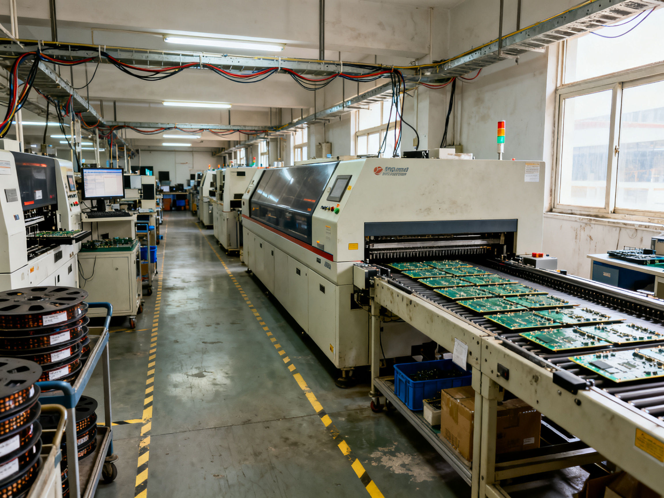
- Incoming inspection. Verify board revision, moisture barrier status, component lots, paste, solder, and flux against the work order. Catches wrong parts and expired or damp material.
- Solder paste printing and SPI. Deposit paste through a stencil, then measure volume, height, area, and offset with solder paste inspection. Catches insufficient or shifted paste that causes bridging and opens.
- Stencil and printer checks. Clean stencils on schedule, verify alignment, and control solder paste temperature and shelf life. Catches paste smearing and aperture clogging.
- Component placement. Pick-and-place for SMT, bench insertion for through-hole parts. Placement accuracy decides whether joints form at all.
- Reflow soldering. The board passes through a lead-free reflow oven on a controlled profile. This is where the surface-mount joints are actually formed.
- Cooling. Controlled cool-down locks the joint microstructure and limits warpage.
- AOI and X-ray. Post-reflow optical inspection finds visible errors; X-ray reveals hidden BGA and QFN conditions. AOI and AXI together are how modern lines close the loop before the board moves on.
- Through-hole joining. Wave soldering, selective soldering, dip soldering, or manual work, depending on the board.
- Cleaning. Remove flux residue and contaminants.
- Test and release. ICT, flying probe, boundary scan, functional test, then packaging with full lot traceability.
| Step | Equipment | Defect it prevents |
|—|—|—|
| Paste printing + SPI | Stencil printer, SPI | Bridging, opens from bad paste volume |
| Placement | Pick-and-place, feeders | Missing, shifted, rotated parts |
| Reflow | Lead-free reflow oven | Cold joints, non-wetting, tombstoning |
| Post-reflow inspection | AOI, AXI | Hidden bridging, voiding |
| THT join | Wave or selective soldering machine | Insufficient fill, bridging, cold joints |
| Test | ICT, flying probe, functional test | Opens, shorts, wrong values |
Where the line gets slow. Work-in-progress piles up wherever the cycle time of one step exceeds the next. On high-volume lines, wave soldering often becomes the serial constraint, because pallet handling, preheat dwell, conveyor transit, and changeovers all add up, while the rest of the line keeps feeding it boards. That is where a wave soldering machine with programmable wave and automated flux handling pays for itself in flow, not just in labor.
Interface points matter too. Most lines mix customer-owned printers, placement, and test equipment with an oven and a wave or selective system from the vendor, so data handoff and recipe governance have to be defined before installation.
Expert Tip: Profile the whole line, not the oven. Takt time is set by the slowest serial step, and inspection capacity downstream of reflow often becomes the real constraint once paste printing is stable.
If you are planning a new line or replacing an aging oven, we can map your takt time and defect history against a proposed configuration. Talk to our team about lead-free reflow ovens, wave soldering machines, and complete SMT production lines.## 3. Reflow Soldering: The Backbone of Surface Mount PCB Assembly
Every surface-mount joint you have ever inspected was born in a reflow oven. Not every PCB assembly needs one, but no high-volume SMT line functions without it, and understanding how it works makes every other process decision easier.
The mechanism, in plain language
Solder paste is a mixture of tiny solder powder particles suspended in flux. The printer deposits it through a stencil as a controlled deposit on each pad. Then the loaded board travels through a lead-free reflow oven on a controlled temperature profile. Flux activates and burns off, the solder particles melt into a liquid, and as the board cools the molten alloy wets the pad and the component termination. Surface tension pulls the liquid into a concave fillet. The component never sees its full melting point directly; only the solder does.
The four zones that decide your defect rate
Profile tuning is where joint quality is really decided. Typical SAC305 guidance from the paste suppliers is a starting window, not a universal standard: roughly 0.5 to 1.5°C per second heating, an optional soak at 120 to 180°C for 60 to 120 seconds, 45 to 90 seconds above the 217°C liquidus, a component peak near 235 to 250°C, and about 2 to 4°C per second cooling, as detailed in this reflow profiling reference from Indium Corporation.
| Zone | What it does | What goes wrong without it |
|—|—|—|
| Preheat and soak | Warms board, parts, and paste gradually; drives off moisture and solvents | Thermal shock, paste slumping, solder balls |
| Active flux | Lets flux do its cleaning job at temperature | Non-wetting, oxidation |
| Peak and soak above liquidus | Melts the alloy fully | Cold joints, incomplete wetting |
| Controlled cooling | Solidifies the joint and locks microstructure | Poor fillet shape, warpage, excess intermetallics |
Terminology and measurement practice for this work are formalized in IPC-7530B, the standard for reflow profiling. Paste datasheets, component temperature limits, laminate construction, and customer drawings always override generic numbers. J-STD-020, often quoted here, is a component moisture classification, not a universal oven recipe.
Choosing the oven type for your board
| Oven technology | Suits best | Watch out for |
|—|—|—|
| Forced air convection | Most production SMT work, mixed board sizes | Cross-width uniformity on wide panels |
| Nitrogen atmosphere | Lead-free, oxidation-sensitive high-density work | Gas cost, leak maintenance |
| Vacuum reflow | BGA, QFN, bottom termination components | Vacuum level, sealing, cycle time |
| Vapor phase | Mixed thermal mass in one load | Solvent cost, throughput |
| Conduction and hybrid | Specialized high-heat or shielded work | Board handling, part compatibility |
On a customer line I profiled last year, the same board passed on a four-zone oven and failed a ten-zone one. The oven was not at fault. The profile was. A low-peak recipe that was fine for the small daughterboard was too aggressive for the heavy chassis, and the fix was zone ramp and soak time, not new hardware.
Where reflow stops working
Reflow joins surface-mount components only. It cannot form through-hole joints. It cannot rework a leaded part reliably, because the whole board would have to go back through the oven. It depends heavily on paste quality, stencil aperture design, and printer calibration, so a bad deposit becomes a bad joint. And it cannot rescue a package with a moisture problem or a pad with poor plating; it can only faithfully reproduce whatever the process gave it.
RoHS lead-free compliance pushes this further. SAC305 peaks near 245°C, which sits close to the limits of some connectors, relays, and older plastic components, so profile validation has to include those parts, not just the smallest package on the board.
If you are upgrading an aging oven or adding reflow capability to a new SMT production line, talk to our engineers about zone count, loaded thermal capacity, and nitrogen or vacuum options for your specific board mix.## 4. The Reflow Soldering Process in Detail: From Stencil Printing to Cured Joints
Most “reflow problems” are actually printing problems. The oven just reveals them.
Before the board ever heats up
Everything that determines joint quality is decided while the board is still cold.
Stencil and aperture design. Aperture area is normally set to about 80 to 90 percent of the pad area for standard components, with more paste for large thermal pads and thermal vias. Aperture shape matters too. Segmented (window-paste) apertures act as a solder reservoir and reduce voiding on QFN and bottom-termination devices, while plain square apertures risk voids and insufficient fill.
Paste selection. Alloy, powder type, and flux chemistry. A no-clean paste still needs a compatible cleaning and inspection plan. Print pressure, speed, and the gap between stencil and board decide whether the deposit lands clean or smears.
SPI. Solder paste inspection measures volume, height, area, and offset before anything is placed. This is the cheapest defect prevention on the whole line, because a bad deposit becomes a bad joint no matter how good the oven is.
Placement. Pick-and-place accuracy is usually quoted at ±0.05 mm or better, but what matters is component-to-pad registration for that specific footprint. Coplanarity on large QFNs, rotation on polarized parts, and seating on bottom-terminated devices cause more cold joints and shorts than most people expect.
The oven journey
- Loading and orientation. Board orientation in the carrier matters for thermal balance and for how the component shadowing works.
- Preheat and soak. The paste’s solvents burn off and the flux activates. Too fast causes thermal shock and slumping; too slow drives out moisture unevenly.
- Liquidus crossing. For SAC305 that is 217°C. Time above liquidus is where the alloy actually flows and wets.
- Peak. Typical windows for lead-free paste run 235 to 250°C for the component peak, and roughly 45 to 90 seconds above liquidus, as published in this lead-free reflow profile supplement from AIM Solder.
- Controlled cooling. Roughly 2 to 4°C per second for SAC305. Fast enough to form a fine grain, slow enough to avoid warpage.
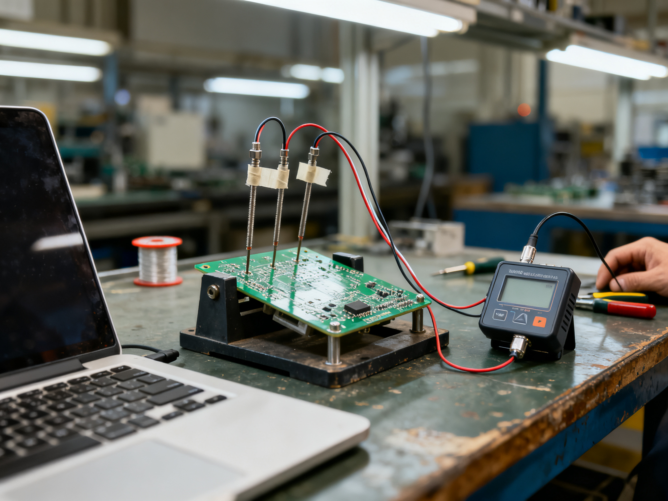
What is actually happening in the joint
While the alloy is molten, copper and tin react and form intermetallic compounds at the pad surface. These layers are strong but brittle. Give them too much time at temperature and they grow thick, and the joint becomes less ductile and more likely to crack.
Cooling rate decides the microstructure. A faster cool produces a finer grain and better fatigue life for BGA standoffs; a slow cool raises warpage and stresses the package. So a joint can look perfect on the bench and still fail in service.
From profile to qualification record
A profile log becomes evidence only when it is tied to the product and the equipment. For automotive and military programs, the record should name the board revision, paste lot, stencil, recipe revision, thermocouple locations, machine ID, profiler calibration date, AOI and X-ray results, deviations, and approvals.
PPAP and FAI packages ask for objective evidence. A signed profile trace, a thermocouple map, and cross-sectioned joints tell the customer far more than a summary slide. Freeze the recipe, re-profile after any oven service, and re-run first article after a paste change. That is what separates a qualified process from a line that happened to work on Tuesday.## 5. Wave Soldering: How the Process Actually Works, and Where It Fails
Picture a conveyor carrying a PCB along the bottom of a long, shallow tank of molten solder. The board’s underside skims the top of a standing wave, gets drenched, and comes out the far side with through-hole pins filled. That is the whole concept. Everything else is detail, but the detail is where the defects come from.
The four stages
- Flux application. Foam flux or a spray head coats the underside of the board. Flux cleans the pads and the component leads, and it must stay active until the joint forms. Apply it too early and it burns off before the solder arrives.
- Preheat. Infrared or convection panels bring the board up toward solder temperature. Preheat matters more than most operators expect, especially on heavy boards and tall connectors. A cold board meeting a hot wave gets a thermal shock, and the result is a joint that looks fine but has a weak, uneven fillet.
- Wave contact. The board enters the wave at a set height and conveyor angle, rides it briefly, then exits. Wave height, contact (dwell) time, angle, and bottom clearance all decide how much solder actually reaches each hole.
- Cooling. The board cools, often with a hot-air knife at the exit to knock off excess solder and stop solder from creeping along the underside.
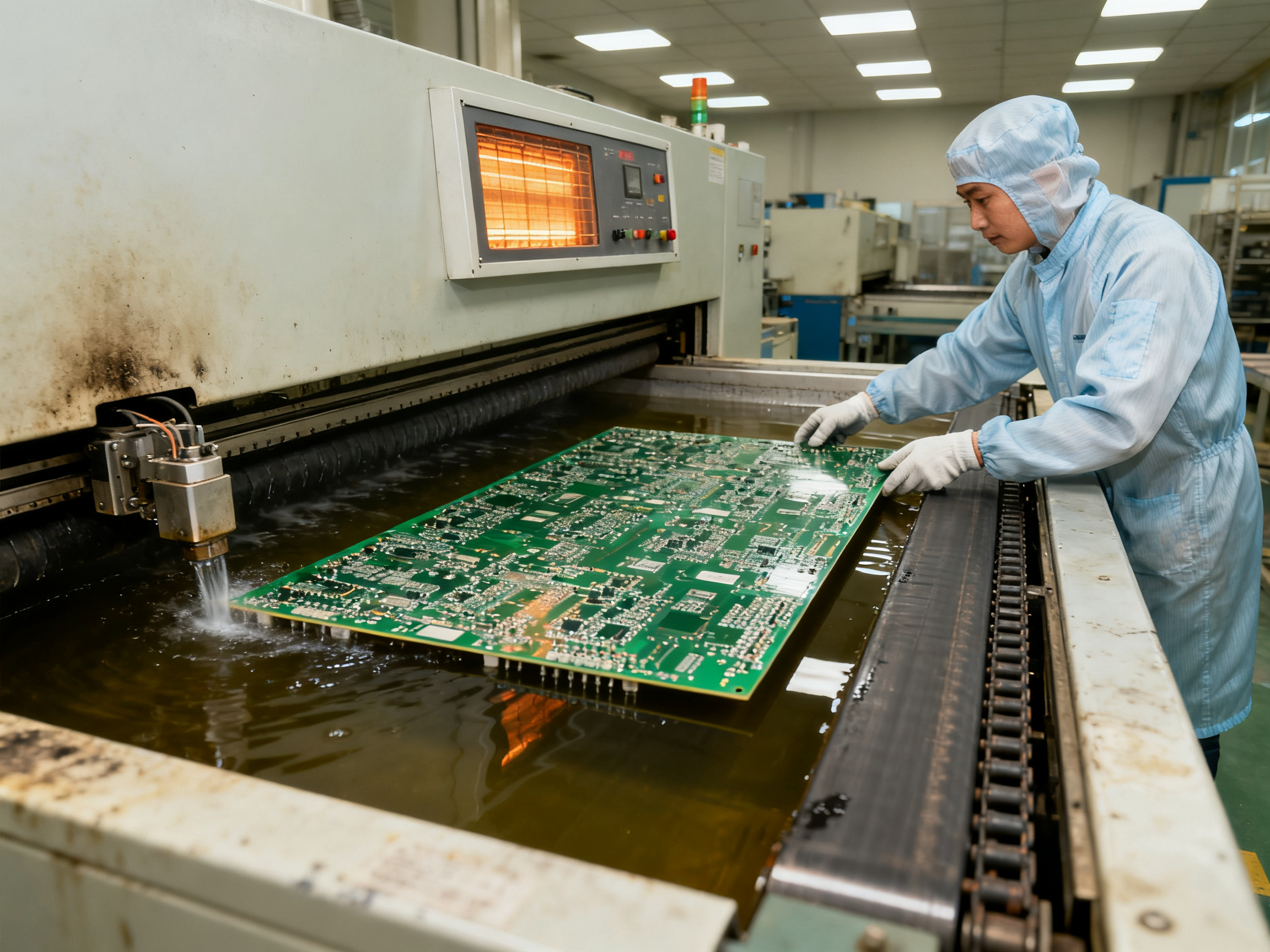
Parameters and the defects they cause
| Parameter | Too low | Too high |
|—|—|—|
| Wave height | Insufficient solder, empty joints, cold joints | Solder splash, bridging, icicles |
| Bottom clearance | Poor drainage, solder wicking into holes | Solder trapped under the board |
| Conveyor angle | No drainage, solder withdrawal marks | Icicles, poor hole fill |
| Preheat | Thermal shock, non-wetting, cracking | Flux burning, paste slumping, component damage |
| Dwell / contact time | Empty joints, insufficient fill | Bridging, solder wicking, thermal damage |
| Solder pot temperature | Cold joints, poor wetting | Dross generation, accelerated oxidation |
Where it fails
Wave soldering is hard to beat for high-volume through-hole work. It joins hundreds of joints in a single pass, costs less per joint than selective soldering, and handles lead-free and high-temperature alloys without drama. That is why it still dominates backplanes, connector assemblies, and power products.
But it fails in predictable ways. Fine-pitch through-hole parts bridge easily because the wave floods everything. Heavy multilayer boards with large copper planes do not preheat evenly enough, so they crack or fill badly. And the solder pot itself is a live variable: it oxidizes, it accumulates dross, and the dross ends up inside joints.
One thing worth flagging for 2026 lines: cleaning the pot is where workers actually get exposed. A NIOSH measurement during a wave machine cleaning task found airborne lead near the OSHA permissible exposure limit. That points at local exhaust, HEPA vacuuming rather than dry sweeping, and segregated waste handling.
Pro Insight: Machine selection decides less than people think. Preheater ramp rate, wave height against board bottom clearance, and pot chemistry with disciplined dross control decide the defect rate. A poorly tuned wave still produces visually acceptable joints, which is exactly why they pass visual inspection and then fail electrical test or cross-sectioning later.
From my own troubleshooting days, the calls I remember best were not mysterious. One was dross build-up in a pot that had not been skimmed for three weeks. Another was a heavy backplane with no preheat, thermal shock on every pass. And one was tombstoning on a row of small resistors right after a conveyor speed change nobody logged. None of those were machine faults. All three were process control.
If your line is running mixed through-hole work and the bottleneck sits at the wave station, we build wave soldering machines with programmable wave and automated flux handling for exactly that reason. Talk to our engineers about your board mix and cycle time.## 6. Dip Soldering: What It Is, How It Works, and Where It Belongs
Think of a pot of molten solder sitting on a heated bench. You dip the leads of a component into it, hold for a second or two, and pull them out. That is a dip solder pot, and it is the simplest way to put solder on a lead. A dip soldering machine does the same thing with controlled bath temperature, immersion depth, dwell time, and withdrawal speed.
Here is the mechanical principle in one sentence: molten solder wets the lead and rises by capillary action, and the fillet left behind is what gives the joint both its mechanical strength and its solderable surface.
The variants you will meet on real lines
- Manual dip pots. A bench pot with a heated bath. Cheap, fast to set up, and entirely dependent on the operator’s timing.
- Motorized or robotic dipping. A machine with controlled depth, dwell, and withdrawal. Repeatable, but still a whole-board or whole-component heat event.
- Lead dipping after insertion. Leads are dipped one at a time or in a gang fixture, often with a solder-mask dam or selective plating to keep solder off body surfaces.
- Dip-and-flux stations for connectors. Common on legacy telecom and power boards where connectors are soldered in bulk.
- Heat-sink and high-current termination. A separate use case in power electronics, where a dipped busbar or lug gets a thick, even coating.
Where dip soldering belongs in modern PCB assembly
Dip soldering is a component-level operation, not a full-board SMT method. It survives in the industry because it is cheap, fast for batches, and it handles the one thing wave and reflow cannot: soldering an individual lead on a board that was never designed to be dipped.
It still shows up on mixed legacy lines, on repair and rework benches, and on low-volume through-hole assemblies where a full wave machine would be overkill.
| Factor | Dip | Wave | Selective | Hand |
|—|—|—|—|—|
| Heat applied to | Whole board or one part | Board underside | Single joints | One joint |
| Joint control | Low | Low | High | Medium |
| Through-hole capable | Yes | Yes | Yes | Yes |
| Fine pitch | Poor | Poor | Limited | Possible |
| Best use | Batched THT, rework, heat-sink attach | High-volume THT | Dense mixed boards | Prototypes, repair |
The honest limitation: because the entire assembly or component takes the heat, board density, component height, trapped air, and thermal sensitivity all constrain what you can safely dip.
Pro Insight: A dip pot is only as good as its bath. Temperature control, flux choice, and contamination monitoring decide the fillet quality far more than the operator’s timing does. Treat the pot as a process to be logged, not a tool to be grabbed.
If your line handles mixed through-hole work and you are weighing a dip station against a wave soldering machine, talk to our engineers about board mix and cycle time before you commit.## 7. Selective, Hand, and Other Soldering Methods Worth Knowing
We have covered the big four separately, so let’s put them side by side and look at what sits outside them. The short version: selective soldering is a robotic cousin of dip soldering, hand soldering is a skill trade, and the rest are niche tools with specific triggers.
Selective soldering
A selective solder machine has a robot moving a nozzle over programmed coordinates, pumping molten solder at specific through-hole joints while shielding the rest of the board. It solves the wave soldering problem where molten solder escapes through holes and flows under nearby parts, and it protects dense undersides and heat-sensitive components that a full board soak would cook. IPC’s technical material on selective soldering for mixed assemblies lays out the same joint-formation logic: heat, dwell time, and component mass are the deciding variables, so there is no universal thermal-mass threshold. This paper from IPC is worth reading before anyone buys a machine on a salesperson’s promise.
On one customer deployment I witnessed, a dense mixed-technology board needed a power connector filled to 85 percent barrel height, but the adjacent aluminum heat sink would have exceeded its temperature limit under a wave pass. Selective was the only route that worked. Reflow plus selective, with a local preheat, did it.
Hand soldering and rework
Hand soldering gets an unfair reputation. With a controlled station, defined joint criteria, good tools, and objective inspection, it can hold up in stable low-volume work. Prototypes, engineering changes, field service, and rework are where it belongs. Realistically, an operator joins a few joints a minute at best, and quality varies with who is on shift, which is the real risk on a high-mix line.
The rest of the toolbox
- Laser soldering. Very local heat, low thermal load, growing interest for fine work.
- Induction soldering. Heats conductive terminals or busbars directly. Fast, and specific to conductive parts.
- Hot dip tinning. Coating a terminal or lug in molten solder for power and heat-sink work.
- Fluxless and reduced-flux processes. Vacuum, formic acid, plasma, or inert atmosphere for high-reliability work where residue is not allowed.
- Conductive and wave-specific alloys. Lower-temperature options that cut thermal exposure, though reliability must be requalified.
Choosing by board type, volume, and mix
| Situation | Sensible route |
|—|—|
| Mostly SMT, high volume | Reflow |
| Many THT joints, wave-safe underside | Reflow plus wave |
| Dense mixed board, heat-sensitive parts | Reflow plus selective |
| Prototype, repair, few joints | Manual |
| Conductive terminals or busbars | Hot dip or induction |
One honest caveat. There is no public study that compares reflow, wave, selective, and hand soldering on identical boards with shared yield and cost definitions. Treat vendor cost claims as directional and demand a like-for-like trial on your own assemblies before signing anything.
Expert Tip: Run a 60-second line audit before you shop. Count your through-hole joints, note how many sit under components, check your annual volume, and list the sensitive parts. That single sheet tells you whether a dedicated wave station, a selective machine, or simply a better reflow oven is the actual gap.
If your line is handling dense mixed boards and you want a second opinion on the process, our engineers at S&M Co. Ltd. can review your board mix and cycle time and tell you plainly whether selective capability is worth the spend.## 8. Reflow vs. Wave vs. Dip: Head-to-Head Comparison for 2026 Production
Ask three engineers which soldering method is best and you get a debate, not an answer. Best for what? That is the whole argument, and the table below is how we settle it on a real line.
| Factor | Reflow | Wave | Selective | Dip / hand |
|—|—|—|—|—|
| Joins | SMT only | Through-hole in bulk | Selected through-hole | Single leads or parts |
| Process window | Wide, profile driven | Moderate, pot and preheat driven | Narrow but precise | Narrow, bath chemistry |
| Typical defects | Bridging, tombstoning, voids | Bridging, insufficient fill, dross | Cold joints, insufficient fill | Uneven fillets, contamination |
| Throughput | Very high | High | Medium | Medium, batched |
| Directional cost per accepted board | $0.50 to $2.00 | $0.30 to $1.50 | $0.60 to $2.50 | $6 to $12 |
| Changeover burden | Stencil, feeders, profile | Pallets, width, flux | Nozzle, program | Minimal |
| Thermal load | Whole board | Underside plus wave | Local only | Whole part |
| Lead-free and high-temp alloys | Proven | Proven, pot care needed | Good, tight control | Good for terminals |
| Best-fit volume | 10,000+ per year | 25,000+ per year | Any volume if mix is dense | Low to medium |
Cost figures are directional supplier estimates rather than audited benchmarks, and they are not comparable unless joint count, labor, tooling, and yield boundaries match. This PCB cost estimating reference walks through why.
Where each method wins
Reflow owns dense surface-mount work. It is the only realistic option for a 100 percent SMT board with BGA and QFN packages, because the whole assembly passes through one controlled profile.
Wave wins on high-count through-hole boards, backplanes, and connector assemblies, where a single pass fills hundreds of joints and cost per joint falls below anything else.
Dip earns its place at component level: busbars, heat-sink terminations, legacy connector work, and repair jobs where no full board can be immersed.
Selective wins the awkward cases: dense mixed-technology boards, heat-sensitive parts, and exposed-pad assemblies that a wave pass would cook.
The line decides, not the method
Nobody buys a soldering machine in isolation. Reflow quality depends on the printer, paste, and SPI upstream. Every method pays for its mistakes downstream in test and rework. Conveyor takt sets the ceiling: if the wave station runs 40 seconds per board and the tester takes 25, you have a bottleneck and a growing queue.
Pro Insight: Most high-volume lines run reflow and wave in parallel and allocate board mix between them. That is a scheduling and takt problem, not a technology contest. Pallet count, material flow, and resource availability can govern effective capacity more than the joining method itself, as this 2026 mixed-line capacity study illustrates.
One honest caveat before you budget from this table. No 2025 or 2026 study compares reflow, wave, selective, and manual soldering on identical boards with shared yield and cost definitions. Published first-pass yield figures cluster around 97 to 98 percent for standard boards and lower for complex automotive or medical assemblies, but those numbers bundle printing, placement, materials, and inspection, so none of them belong to the soldering step alone. Treat any head-to-head cost claim as directional until you run a like-for-like trial on your own boards.## 9. Defects, Quality Control, and Traceability: Where Soldering Methods Fail
Every method fails in its own recognizable way. Reflow gives you bridging, tombstoning, and hidden voiding under fine-pitch packages. Wave gives you bridging, short barrel fill, dross, and icicles. Selective gives you cold joints and localized burns. Manual gives you operator variation. That defect list is the real fingerprint of the process, and reading it correctly tells you where to look.
| Defect | Root cause | Method that shows it most |
|—|—|—|
| Bridging | Excess or shifted paste, wave height too high | Reflow and wave |
| Insufficient solder | Low paste volume, short dwell, poor wave contact | Reflow, wave, selective |
| Tombstoning | Thermal imbalance on small terminations | Reflow |
| Head-in-pillow | Package or board warpage, oxidation, poor coalescence | Reflow on BGA |
| Voiding | Outgassing, stencil aperture shape, trapped flux | Reflow on QFN and bottom-termination |
| Cold joint | Low temperature, contamination, wrong flux | Wave, selective, manual |
| Barrel fill under 50 percent | Dwell too short, preheat too high, wrong board angle | Wave and selective |
| Icicle and solder splash | Withdrawal behavior, wave turbulence | Wave |
| Burn or heat damage | Excessive thermal exposure | Dip, wave, selective, manual |
The inspection stack has to be an evidence chain
Each technology proves something different, and none of them proves everything.
- SPI measures paste volume, height, area, and offset before placement. It cannot prove reflow wetting, but it is the cheapest defect prevention on the line.
- AOI finds visible presence, polarity, alignment, bridges, and fillet problems. It stays line-of-sight, so it cannot see under a package.
- X-ray and CT reveal bridging, voids, and missing solder inside BGA and QFN bodies. Projection overlap can hide or mimic defects, and CT is slower, so both are qualification and failure-analysis tools more than everyday gates.
- Cross-sectioning is destructive and sample-limited, but it is the only way to see intermetallic growth and true internal geometry.
- Boundary scan and electrical test prove behavior, not morphology. A weak joint can pass electrically and still fail in service.
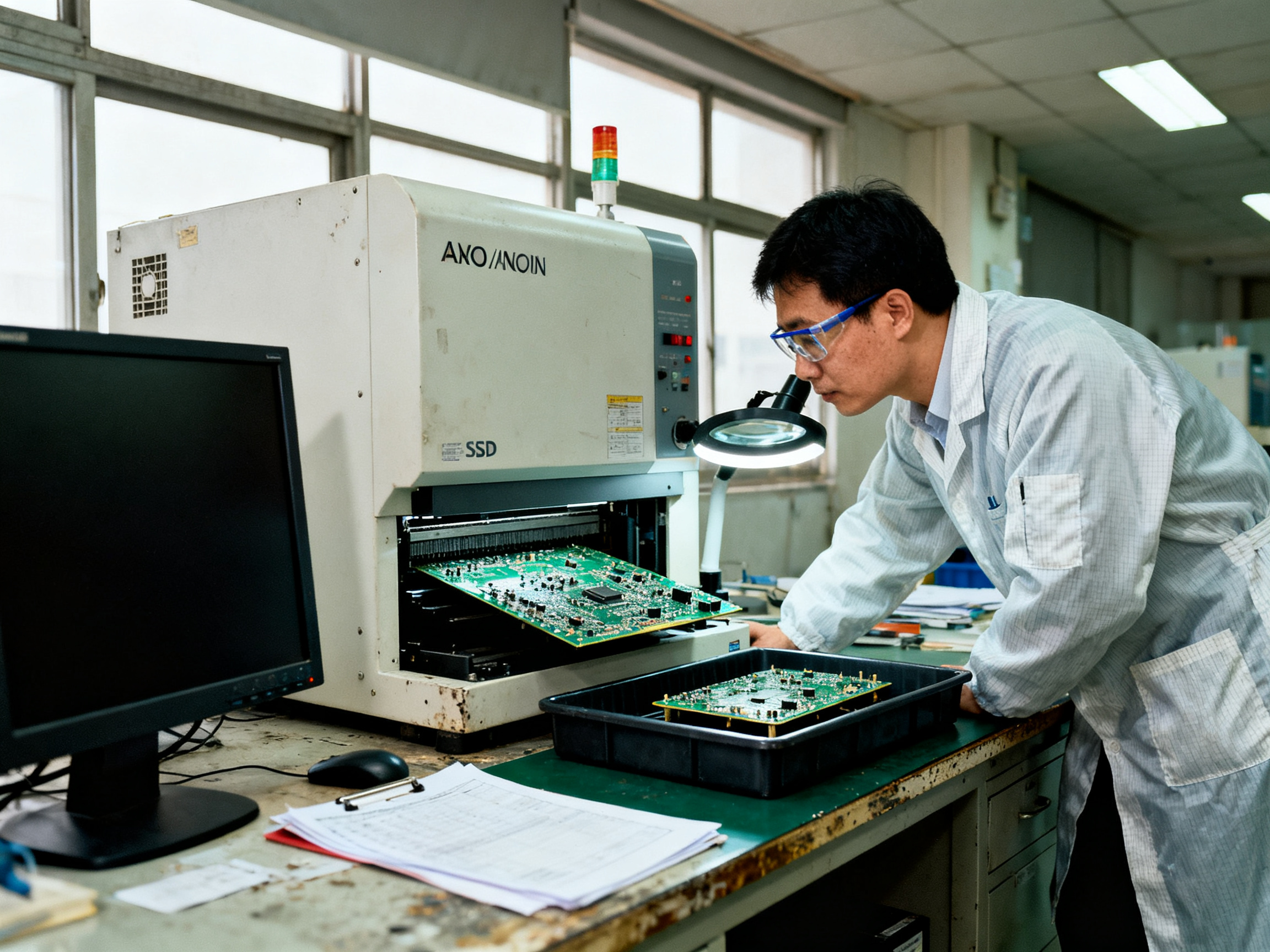
Method choice drives inspection cost
Visible through-hole joints are cheap to check. Hidden joints under a 0.4 mm BGA are not. That is why the inspection budget should follow the joint, not the board count. Expect AI-assisted AOI to help with triage, but judge it per defect class rather than by headline accuracy, since published work reports solid performance on easy classes and much weaker precision on difficult ones after high false-positive counts (2025 AOI study, MDPI).
On one line I reviewed, a head-in-pillow call from X-ray looked like a placement problem. Cross-sectioning showed the real cause: a warped BGA package sitting on a heavily populated board, with oxidation between the ball and the paste. No amount of profile tuning would have fixed it. The fix was a change in package supplier and a reworked carrier.
Traceability is what turns a defect into a fix
A defect rate without a denominator is decoration. Record the boards presented, the first-pass yield against that population, and the defect Pareto by method and machine. Then connect each defect to its material lot, stencil, recipe revision, profile trace, and inspection result. Without that chain, you are guessing.
The cost of quality follows the same chain. Rework minutes multiply by loaded labor and add up faster than most shops expect on high-volume consumer lines, and scrap on a mixed board can exceed the cost of the soldering step itself. Fixing the process upstream is always cheaper than catching the defect downstream.## 10. Choosing the Right Soldering Method: A Decision Framework for Manufacturers
Choosing a soldering method is mostly a matter of counting things properly before you spend anything.
Step 1: Collect the inputs
- Board mix: share of SMT versus through-hole, joint count, hole size, pad geometry
- Packages: BGA, QFN, LGA, connectors, heat sinks, transformers, relays
- Board construction: dimensions, layer count, copper planes, thermal mass
- Volume: annual quantity, batch size, number of variants, changeover frequency
- Compliance and quality class: RoHS exposure, IPC-A-610 class, customer drawing
Step 2: Route it
| Product profile | Sensible route in 2026 |
|—|—|
| 100 percent SMT, fine pitch, high volume | Multi-zone convection reflow, nitrogen optional |
| Mixed THT and SMT, high volume, wave-safe underside | Reflow plus wave |
| Mixed board, thermal-sensitive parts, exposed pads | Reflow plus selective soldering |
| Conductive terminals, busbars, terminations | Hot dip or induction |
| Prototype, engineering change, repair | Manual with controlled station |
Step 3: Judge the equipment, not the label
Zone count alone is a weak proxy. What matters is usable heating and cooling length, loaded thermal capacity, cross-width uniformity, conveyor options, recipe management, data export, alloy support, protocol compatibility with your MES, and local spares and service. For wave and selective lines, look at preheat capability, flux application, pot and nozzle condition, dross handling, and cycle time on your own board geometry.
Step 4: Frame the ROI honestly
Use accepted-board cost: (setup, tooling, changeovers, variable processing, maintenance, rework, and scrap) divided by quantity times first-pass yield. There is no public benchmark that gives you a universal payback period for an oven upgrade or a selective machine, so build the model with your own labor, energy, and scrap numbers, then sensitivity-test it.
Expert Tip: Run a 60-second line audit before you shop. Count through-hole joints, note how many sit under components, check annual volume, and list your heat-sensitive parts. That one sheet tells you whether you actually need a wave station, a selective machine, or simply a better reflow oven.
In past consumer-electronics installations, the answer was often a four-zone to ten-zone reflow oven plus a conveyor speed change, and the takt gain from the oven was larger than anything a new wave machine would have delivered. So sizing the oven zones and conveyor takt against your real product mix first is the cheapest step in the whole project.
If you want a second opinion before you build a business case, our engineers at S&M Co. Ltd. can review your board mix, volume, and cycle time and tell you plainly whether new equipment is justified, and which one.## Conclusion: Key Takeaways and Next Steps for Manufacturers
The pcb assembly process is a chain, not a single event. Every step needs to catch its own failures before the next one hides them, and the soldering method is the biggest lever you control on defect rate, thermal stress, and compliance. Reflow handles surface-mount work. Wave handles high-volume through-hole. Dip, selective, and manual cover targeted and low-volume cases.
From Our Experience: Three upgrade triggers have consistently justified new equipment on customer lines: lead-free profile capability on older ovens, BGA and QFN density that demands better inspection and profile control, and a wave station that has become the takt constraint. Two common false triggers do not: “our competitors bought one” and “we want more zones.” Zone count alone tells you very little about loaded thermal capacity or cross-width uniformity.
Here is the order of operations I’d follow tomorrow morning:
- Audit the line by method and defect category. Sort your last quarter of defects by joining method, then by root cause. The biggest bucket is usually your next project.
- Define the target mix and quality class. Board construction, throughput, rework cost, and the acceptance standard from the contract or drawing.
- Shortlist equipment against the framework, then run an acceptance trial on real production boards with frozen metrics: first-pass yield, cycle time, rework minutes, and changeover time.
For consumer electronics, the priority is throughput and stencil-to-reflow repeatability. Semiconductor and automotive work lives or dies on BGA and QFN joint quality plus traceability. Military and aerospace programs need frozen recipes, signed profile traces, and retained records.
If you want a second opinion before you build the business case, our engineers at S&M Co. Ltd. will review your board mix, volume, and cycle time, and tell you plainly whether new equipment is justified and which one.
Related reading: What is PCB assembly? | Reflow vs. wave soldering compared | Dip soldering explained | Defect and traceability guide