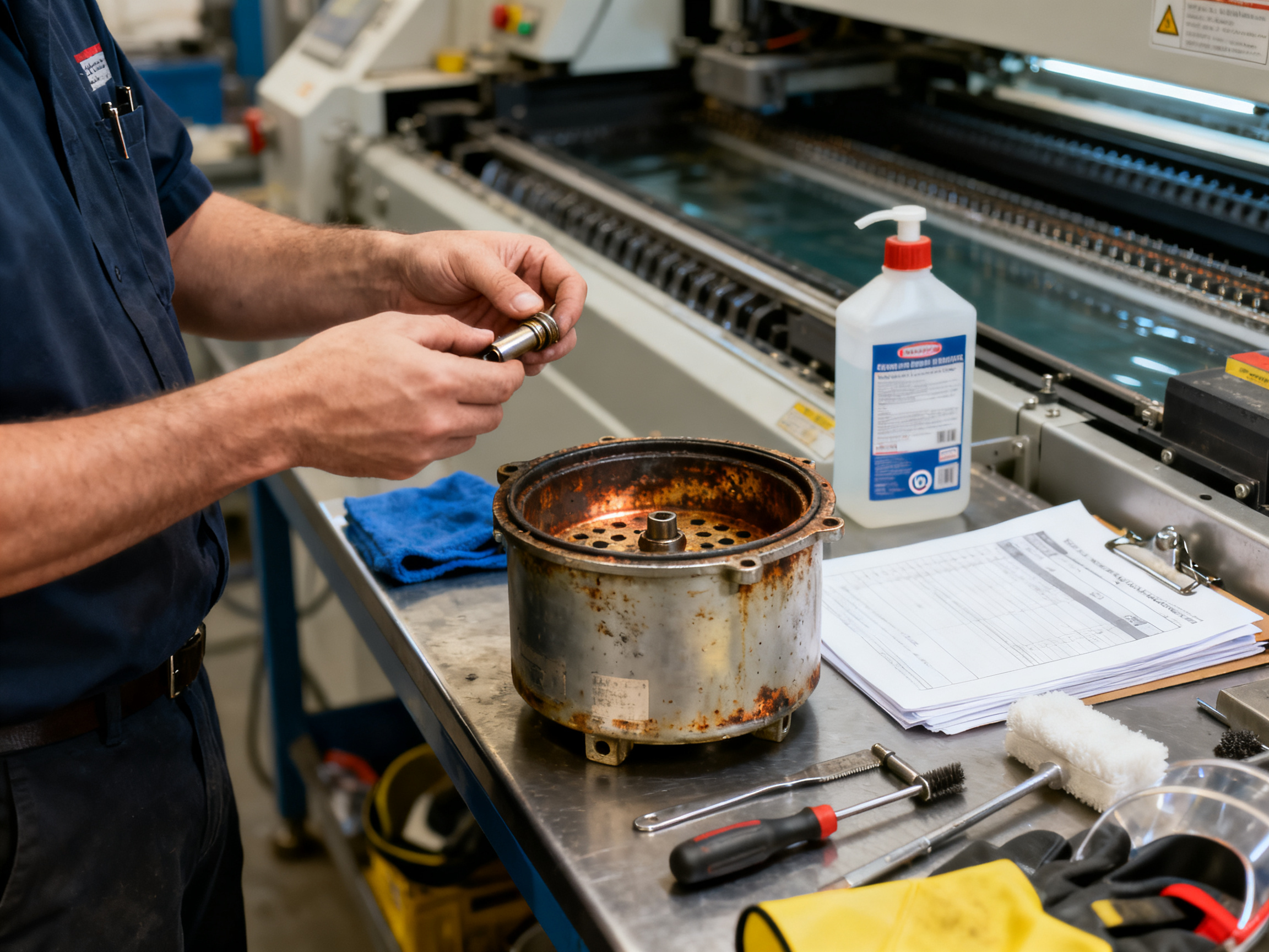
Published: 23 September 2026
Reading Time: 18 minutes
Reviewer: Simon Scrapes, Founder
Introduction: The Critical Role of Wave Soldering in Modern Electronics Manufacturing
Picture this. It’s a Tuesday morning in your assembly facility, and your wave soldering line is running at full speed. Suddenly, you notice bridges forming between joints on one of your boards. Before you know it, you’re facing an hour of rework and your production targets are slipping. Sound familiar?
You’re definitely not alone. In high-volume manufacturing, the wave soldering process flow can make or break your entire operation, and when something goes wrong, the ripple effects hit your bottom line hard.
Wave soldering remains a cornerstone technology for through-hole PCB assembly in 2026. Even as selective soldering has gained ground for mixed-technology and high-density boards, wave soldering still handles the highest throughput where through-hole components dominate. Industry data suggests approximately 65% of large-scale PCB manufacturing facilities depend on wave soldering as their primary through-hole assembly method. The global wave soldering equipment market reflects this sustained demand, with projections showing growth from $1.8 billion in 2025 to $3.1 billion by 2034.
So why does this matter for you and your team?
Here’s the thing. Wave soldering is straightforward in concept, but it demands precise control in practice. Small deviations in wave height, conveyor speed, preheat temperatures, or solder bath composition can trigger defects that slow your line and tank your first-pass yield. We’re talking about issues like bridging between adjacent joints, icicles hanging off pad edges, incomplete hole fill, or pads that simply won’t wet properly.
This guide gives manufacturing professionals like you a complete walkthrough of the wave soldering process steps, from flux application through preheating, wave contact, cooling, and final inspection. We’ll cover the temperature profiles that work best, the common defects that plague high-volume lines, and the practical fixes that actually move the needle.
Whether you’re fine-tuning an existing line, troubleshooting recurring problems, or setting up your first wave soldering operation, you’ll find actionable insights here. Let’s get into it.## The Wave Soldering Process: How It Works
Let’s get into the actual mechanics. How does a wave soldering machine actually create those reliable joints we’re after?
At its core, wave soldering is pretty elegant. A pump pushes molten solder upward through a nozzle, forming a controlled, continuous wave that looks almost like a static ribbon of liquid metal. The PCB rides on a conveyor and passes over this wave, with its underside making contact. That’s the moment where the magic happens.
The conveyor system does a lot of the heavy lifting here. It controls three critical things simultaneously: the angle of the board relative to the wave, how fast the board moves through, and how deep the board dips into the wave. Most setups run the board through at a slight angle, usually between 5 and 7 degrees. That angle matters because it affects how the solder peels off the board at the exit point, and believe me, that peel-off behavior is where a lot of defects either get made or avoided.
Here’s what most people don’t think about. The wave itself isn’t flat. Modern machines use shaped nozzles to create a wave with a specific curvature, which helps the solder flow smoothly across the board and drain properly at the tail end. The height of that wave matters too. Get it too high and you’re drowning your components, too low and you won’t get proper hole fill.
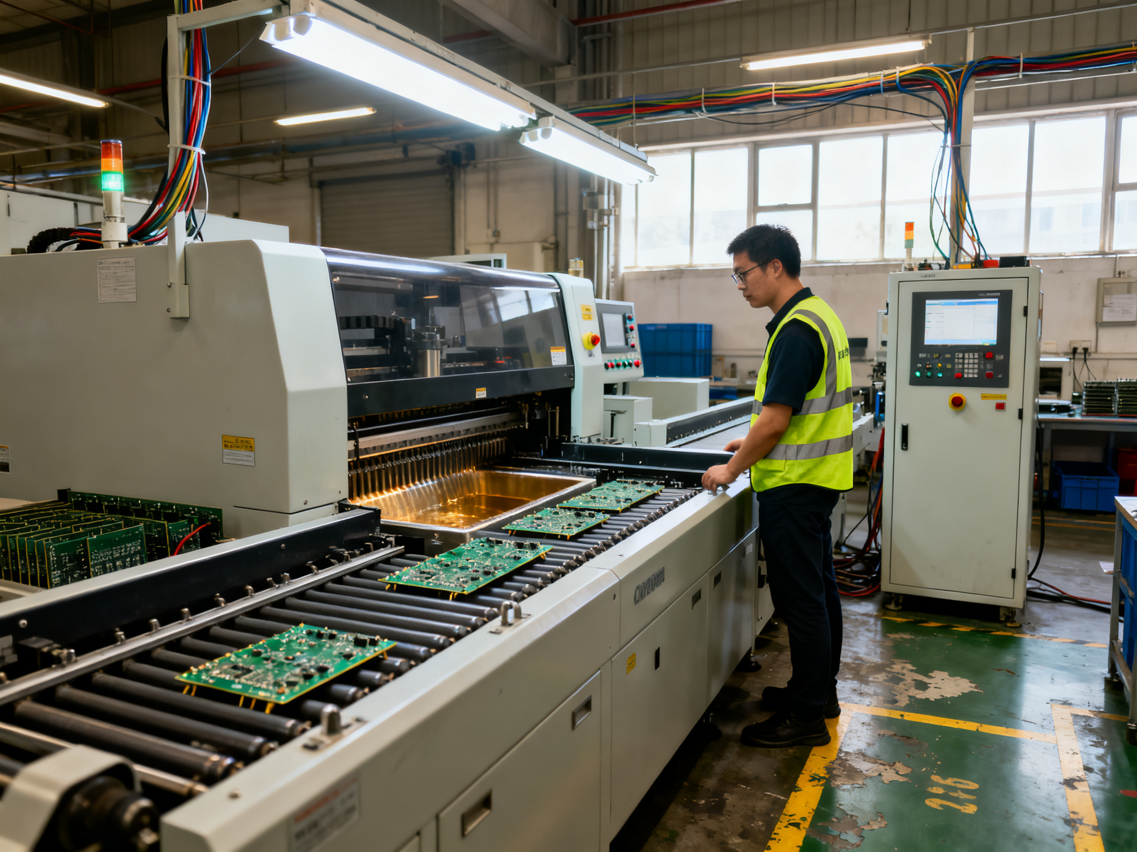
A typical wave soldering machine strings together several stages in one continuous line. First comes flux application, then preheating to bring the board up to temperature gradually, then the solder wave itself, and finally cooling to solidify those joints before they go to inspection.
From Our Experience:
We’ve watched operators dial in everything perfectly during setup, then watch defects mysteriously appear three hours later. Usually, it’s the small things: flux density drifting as it evaporates, wave height settling as the pot cools slightly, or conveyor belt tension changing after warm-up. The process looks simple on paper, but keeping it consistent over a full shift takes active monitoring, not just initial setup.
Each stage feeds into the next. Flux readies the surfaces for wetting. Preheat drives off moisture and activates the flux chemicals while preventing thermal shock. The wave provides the actual solder contact. And cooling lets the joints solidify with the right microstructure. Miss any of these and you’ll feel it in your defect rates.
Modern machines also include monitoring systems that track temperatures, conveyor speed, and flux delivery automatically. Some connect directly to MES systems for real-time traceability, which is becoming a bigger deal as customers demand more documentation of your process controls.
[Technical illustration showing wave soldering machine cross-section with labeled components: conveyor system, fluxer, preheat zones, solder pot with pump and shaped nozzle, cooling section, and direction of PCB travel]
Understanding this flow helps you see why changing one parameter often affects others. Tighten your conveyor speed and you change contact time, which affects how much heat the board absorbs from the wave. It’s all connected.## Understanding the Wave Soldering Process Steps
Here’s where we get into the meat of it. The wave soldering process flow isn’t just one big step. It’s actually a chain of seven distinct stages, and each one matters if you want joints that pass inspection the first time.
Let’s walk through them.
Stage 1: Flux Application
Flux readies the metal surfaces. It cuts through oxides on the pads and component leads, so solder can actually wet properly. Without good flux coverage, you’re fighting an uphill battle against poor wetting and skips. Machines apply flux via spray or foam systems, and the deposit needs to be thin and even across the board underside.
Stage 2: Preheat
The board warms up gradually. This drives off moisture, activates the flux chemicals, and gets everything ready for the molten solder. Too cold and the flux won’t work right; too hot and you risk damaging components or creating solder balls. We typically target a topside temperature around 100 to 150 degrees Celsius for lead-free work.
Stage 3: Wave Contact
This is the main event. The PCB rides over the solder wave at a controlled speed, angle, and immersion depth. Capillary action pulls solder up into the plated through-holes. Contact time usually runs about 2 to 4 seconds, depending on the board and alloy.
Stage 4: Cooling
Joints solidify after wave exit. Controlled cooling matters because it affects grain structure and thermal stress in the assembly. Rush this step and you’ll feel it later in field failures.
Stage 5: Cleaning
Flux residues come off chains, nozzles, and machine surfaces. Depending on your flux type, you might also need to clean the boards themselves to remove any remaining residue.
Stage 6: Inspection
Visual checks catch bridges, icicles, and obvious wetting problems. AOI systems help with repeatable defect detection across high volumes.
Stage 7: Rework
Any defective joints get repaired before the board moves downstream. This is your safety net, but it shouldn’t be your primary quality strategy.
From Our Experience:
We’ve seen lines where operators treat rework as normal. After a while, they stop asking why defects keep appearing and just work around them. That’s a slippery slope. Rework has its place, but if you’re reworking more than a few percent of your boards, something upstream needs fixing.
Here’s the thing though. These stages don’t exist in isolation. They flow into each other like links in a chain.
Flux that doesn’t activate properly in preheat creates problems at the wave. Wave contact that’s too brief leads to insufficient hole fill, which cleaning and inspection will expose. And cooling that’s too rapid can induce stress fractures you’ll only see in thermal cycling tests later.
The conveyor ties everything together. It sets your contact time, determines how much heat the board absorbs from the wave, and controls the angle at which the board exits. Change one variable and the others feel it.
Modern equipment handles most of this automatically, tracking temperatures, conveyor speed, and flux delivery in real time. Some systems log everything to MES for traceability, which customers increasingly expect.
Most wave soldering in 2026 uses lead-free alloys like SAC305. This means higher pot temperatures and tighter process windows than the old tin-lead days. SAC305 typically runs around 260 to 280 degrees Celsius at the wave, with conveyor speeds around 1.0 to 1.5 meters per minute for single-wave setups.
The good news? Once you understand how these seven stages connect, you can tune your line for consistency and keep it there.
Step 1: Flux Application and the Role of Wave Soldering Flux
Flux comes first in the wave soldering process flow, and honestly, it’s the foundation that makes everything else possible.
Think of flux as your preparation layer. It removes oxides and contaminants from your PCB surfaces, leaving clean metal that solder can actually bond to. Without good flux coverage, you’re fighting an uphill battle against poor wetting and skipped joints from the get-go.
Beyond cleaning, flux protects against new oxidation forming during the heating phase and helps solder spread evenly across the board. That’s a lot of heavy lifting from what looks like a simple chemical coating.
Flux Types and What They Do
Three main flux types dominate wave soldering in 2026:
Rosin-based fluxes are the most forgiving on slightly contaminated surfaces. They deliver solid wetting performance but often leave residues that need cleaning afterward.
Water-soluble fluxes are more active and clean better after aqueous washing. The tradeoff is that any cleaning miss leaves corrosive residue behind, so process control matters here.
No-clean fluxes minimize residue and work for general production without post-solder cleaning. They’re a popular choice where cleaning steps add cost or complexity.
These categories follow IPC/J-STD-004B classification with codes like ROL0, ORL0, ORH0. The letters tell you the base chemistry (rosin, organic, or resin), and the number indicates activity level.
How Flux Gets Applied
Application method matters as much as flux type. Spray application gives the best control and uniform coverage, making it the standard for modern production. Foam fluxing works for simpler boards with lower component density, but it requires more maintenance attention. Fountain application delivers aggressive wetting but risks carrying excess flux onto the board if parameters aren’t tightly managed.
| Flux Type | Residue | Cleaning Required | Best For |
|———–|———|——————-|———-|
| Rosin-based | Yes | Often required | General through-hole assemblies |
| Water-soluble | Yes | Yes (aqueous wash) | High-reliability boards |
| No-clean | Minimal | No | Standard production runs |
Why Deposit Control Matters
The amount of flux deposited directly ties to your defect rates. Too little flux causes poor wetting and skips. Too much leaves residues that create reliability concerns or demand extra cleaning steps.
Modern no-clean fluxes often run just 1.85-4% solids, reflecting the industry’s push toward lower residue formulations without sacrificing wetting performance.
Environmental and safety considerations shape flux choice in 2026 too. Water-soluble and no-clean options dominate due to VOC regulations and worker safety requirements. Lead-free soldering’s higher process temperatures also influence flux compatibility with specific alloys, so always verify your flux works with your solder chemistry.
Bottom line: flux application isn’t a step to gloss over. Get it right and your wave contact stage has every chance of success. Get it wrong and you’ll spend the rest of your shift chasing defects.
Step 2: Preheating Stage: Achieving Optimal Thermal Equilibrium
Here’s where a lot of operators cut corners, and honestly, it’s usually because preheat feels invisible. Unlike the solder wave, there’s no dramatic molten metal action to watch. But the preheating stage sets up everything that happens next, and skipping it or doing it wrong will cost you in defects every single time.
The preheat zone does three jobs at once. It drives off any moisture that’s settled on the board since reflow. It activates the flux chemicals so they can do their job at the wave. And it brings the entire assembly up to temperature gradually, so meeting molten solder doesn’t shock your components.
That last point matters more than people realize. If your board comes straight from a cool room and hits 260-degree solder, the thermal stress can crack ceramic capacitors, delaminate board layers, or cause hidden internal defects that show up weeks later in the field. Nobody wants that conversation with a customer.
Typical topside preheat targets run around 100 to 150 degrees Celsius for lead-free work. You want to avoid exceeding about 150 degrees Celsius difference between your preheat exit temperature and your solder wave temperature. Cross that threshold and you’re asking for thermal shock problems.
The ramp rate matters too. You’re aiming for something gentle, usually under 3 degrees Celsius per second during the ramp-up phase. Slamming the board with heat creates temperature gradients across the assembly, and those gradients cause uneven expansion that leads to warpage, component stress, and defects downstream.
So how do different boards behave? Here’s the quick rundown:
| Board Type | Typical Preheat Target | Considerations |
|————|———————-|—————-|
| Thin boards (<2mm) | 100-120°C topside | Heat absorbs quickly, easy to overshoot |
| Standard boards (2-3mm) | 110-140°C topside | Most forgiving range |
| Thick boards (>3mm) | 130-150°C topside | Needs more heat input, longer preheat zone |
| High-copper-density boards | 130-150°C topside | Copper pulls heat, harder to bring up uniformly |
We notice that boards with heavy copper planes or large thermal masses often need extended preheat time. The thermocouples on your hottest and coldest joint locations tell you if you’re actually achieving equilibrium, not just hitting a target temperature on one spot.
Modern machines give you multiple preheat zones you can tune independently. This flexibility helps when you’re running boards with mixed thermal masses, like a big connector next to a small resistor array. You can dial back the heat under the dense area while making sure the thinner sections still hit their target.
The payoff for getting preheat right? Better hole fill, fewer skips, reduced solder balls, and less stress on your components. It takes a few minutes to profile properly, but it pays dividends across your entire production run.
Step 3: The Soldering Wave: Contact, Wetting, and Transfer
This is where the magic actually happens. After all the prep work with flux and preheat, your board meets the molten solder wave, and those joints form in just a few seconds of contact.
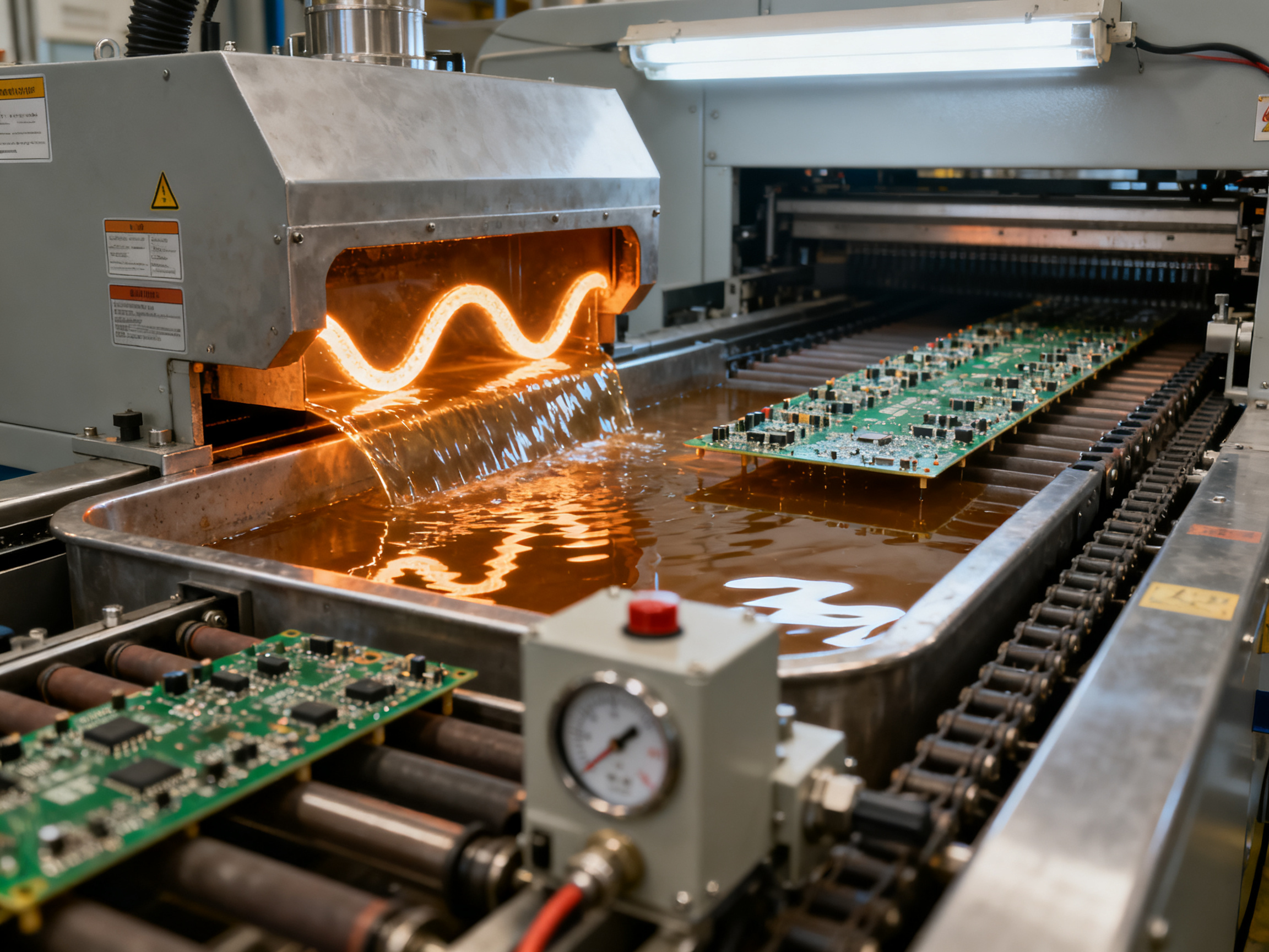
The wave itself is generated by a pump pushing solder through a shaped nozzle. That nozzle design matters more than most people realize. It creates a wave with a specific curvature that helps solder flow smoothly across your board and drain cleanly at the exit. Get the wave shape wrong and you’ll deal with turbulence, solder splashing, or uneven coverage across the board.
Wave height sits as a starting point at about half to two-thirds of your board thickness for single-wave setups. Too high and you drown your components and create bridges. Too low and you won’t get proper hole fill in your through-holes. The sweet spot depends on your board thickness, component density, and pad geometry.
Contact time with the wave typically runs around 2 to 4 seconds for most lead-free setups. IPC J-STD-001 Revision H (2026) specifies 3 to 5 seconds for wave soldering applications. Longer contact means more heat input and better hole fill, but it also increases thermal stress on your components and raises your risk of icicles forming at the exit point.
Conveyor angle works alongside speed to control how the board peels away from the wave at the end of contact. That peel-off point is where bridges and icicles get made or avoided. Most lines run at 5 to 7 degrees, but the right angle depends on your board design and what defects you’re fighting.
Now here’s something nobody talks about enough. Your solder bath composition drifts over time. Copper leaches from boards into the pot, especially with lead-free SAC305 alloys. Zinc and other impurities accumulate. All of this changes how the solder wets and flows. Regular bath analysis matters because contaminated solder doesn’t behave like fresh solder, even if your temperatures and speeds look correct on paper.
The dross layer on top of your pot is another culprit. That oxide layer insulates the solder and interferes with heat transfer. Remove it regularly, usually once per 8-hour run, and keep your pump and nozzle surfaces clean. Poor bath condition connects directly to excess bridging and icicling.
When the board exits the wave, capillary action has pulled solder up into the plated through-holes. That fill action depends on everything working together: clean surfaces from proper fluxing, adequate heat from preheat and wave contact, and good wetting from healthy solder chemistry. Miss any link in that chain and your hole fill suffers.
Pro Insight:
We’ve tracked solder bath contamination across dozens of production runs. Copper levels climbing past 1.0% in SACX alloys consistently show up as wetting problems 2 to 3 hours before operators notice defects on the board. If you’re waiting to see bridges before checking your pot, you’re already behind. Set up a bath analysis schedule and stick to it.
The wave parameters you set during setup, wave height, conveyor speed, contact time, and angle, all interact with each other. Tighten your speed and you reduce contact time. Raise your wave and you increase solder volume on the board. These aren’t independent knobs. Change one and you’ll need to evaluate whether the others still make sense for your board.
For SAC305 lead-free work in 2026, you’re typically running your pot at 255 to 265 degrees Celsius with conveyor speeds around 1.0 to 1.4 meters per minute. Those are starting points though. Your specific board thickness, copper weight, and component thermal mass will tell you if you need to adjust from there.
## Step 4: Cooling and Solidification of Solder Joints
Here’s a stage most people rush through without giving it much thought. Your board exits the wave, looks perfect, and moves on. But what happens in the seconds after wave contact determines whether those joints hold up for years or fail prematurely in the field.
Cooling is where the solder transforms from liquid to solid, and that transition matters a lot. Get it right and you get joints with fine grain structure and good mechanical strength. Rush it and you’ll create thermal stress that shows up as cracks, delamination, or field failures you won’t see until months later.
Why Cooling Rate Hits Your Bottom Line
The rate at which your joints cool affects the intermetallic layer that forms between the solder and the copper pad. This layer is what actually holds the joint together. Cool too quickly and the intermetallic can be uneven or overly thick. Cool too slowly and you risk coarse grain structure that weakens the joint.
For SAC305 lead-free alloys, we’re talking about solidification starting around 217 to 219 degrees Celsius. The goal is to let that cooling happen in a controlled way without shocking the assembly with cold air or uneven temperatures.
The thermal gradient across your board during cooling matters too. If one side cools faster than the other, the board can warp slightly. That warpage might not be visible, but it puts stress on joints and components that builds up over thermal cycling.
What Actually Works in Practice
Most wave soldering machines have dedicated cooling zones with controlled air flow. The key is matching that cooling to your board characteristics.
Thin boards cool faster naturally. You might need to dial back the cooling intensity or add some preheat overlap to avoid creating temperature gradients. Thick boards with high copper content act like heat sinks, pulling heat away slowly. They often need more aggressive cooling to hit the right solidification profile.
We’ve found that monitoring the board topside temperature as it exits the cooling zone gives you a good indicator of whether your cooling is balanced. Most shops target a board temperature somewhere around 100 to 120 degrees Celsius at the cooling zone exit, but your specific board thickness and thermal mass will determine where you need to be.
Expert Tip:
When you’re profiling a new board, put thermocouples at the corners and center of the board, not just near joints. Uneven cooling often shows up at the board edges first. If you see temperature differences greater than 15 degrees Celsius across your board during cooling, adjust your cooling zone air flow before you run production.
The air flow direction and velocity in your cooling section should be consistent across the board width. Dead spots or turbulent areas create temperature variations that translate directly into quality variations across your production.
The Connection to Everything Else
Here’s the thing. Cooling doesn’t exist in isolation. Your cooling zone performance is only as good as your preheat. If you brought the board up unevenly, you’ll see those same patterns when it cools. The whole thermal journey from flux application through cooling needs to be treated as one connected process.
Board support matters as well. If your conveyor belt or pallet doesn’t support the board flat during cooling, gravity and thermal stress combine to create warpage. We always check board flatness at the cooling zone exit as part of first-article verification.
When your cooling is optimized, you get joints that pass thermal cycling tests, hold up under vibration, and look consistent under inspection. When it’s off, you’re basically rolling the dice on field reliability.
Proper cooling sets the stage for your final inspection stage. Get it right and your boards move through QC cleanly. Get it wrong and you’ll spend time chasing stress-related failures that don’t show up until much later.
Wave Soldering Temperature Profile: The Key to Consistent Quality
Here’s something we see all the time in manufacturing facilities. Two lines running the same board, same solder alloy, same machine brand. One line hits 95% first-pass yield. The other struggles to hit 80%. What’s the difference?
Usually, it’s the temperature profile.
The temperature profile isn’t just one setting. It’s the entire thermal journey your board takes from the moment it enters the preheat zone until it finishes cooling. Every degree and every second adds up, and getting this right separates consistent production from constant firefighting.
What Goes Into a Temperature Profile
Think of your profile as a recipe. It includes your solder pot temperature, your preheat zone temperatures, how fast your conveyor moves, how long the board contacts the wave, and how quickly it cools after. Miss any of these ingredients and your results suffer.
For SAC305 lead-free work in 2026, your solder pot typically runs around 255 to 265 degrees Celsius. Your preheat zones should get the board topside to about 100 to 150 degrees Celsius before it hits the wave. That preheat-to-wave gap should stay under 150 degrees Celsius or you risk thermal shock that cracks components and delaminates layers.
Conveyor speed usually sits around 1.0 to 1.5 meters per minute for single-wave setups. Faster speed means shorter contact time with the wave. Slower speed means more heat input and better hole fill, but also more stress on your components.
IPC-7530 recommends keeping your Time Above Liquidus (TAL) between 60 and 90 seconds for SAC305 alloys. That’s the window where your solder stays molten enough to wet properly and fill those through-holes. Too short and you get skips. Too long and you risk intermetallic overgrowth that weakens joints.
Balancing the Three Big Variables
The trickiest part of profiling is that these parameters interact with each other. Change your conveyor speed and you change contact time. Change your wave height and you change how much heat transfers to the board. Raise your pot temperature and you affect dross formation and flux performance.
Board thickness throws another wrench into the works. We noticed that thinner boards heat up faster during wave contact than thicker ones, even with identical pot settings. A 2.4mm board can run significantly hotter than a 5.0mm board using the exact same profile. That’s why profiling with actual thermocouples on your specific board matters so much.
Copper density on your board also changes everything. Heavy copper planes pull heat away from joints, creating uneven thermal gradients across the panel. You might profile for your densest area and then discover your thinner sections are overheating.
Modern Profiling Tools
Here’s the good news. Wave soldering machines in 2026 come with profiling software that makes this a lot less guesswork. You place thermocouples at key locations on a test board, run it through the process, and the software captures the actual temperature curve at each point.
IPC-7530 recommends placing thermocouples at your highest thermal mass location (think large connectors or BGAs) and your lowest thermal mass location. You want to make sure both ends of the thermal spectrum hit acceptable windows.
Modern systems also include real-time monitoring that tracks pot temperature, preheat temperatures, conveyor speed, and flux delivery automatically. Some connect directly to MES systems so you have complete traceability for every board that runs through.
Expert Tip:
When profiling boards with mixed thermal masses, put thermocouples at the corners and center of the board, not just near joints. Uneven cooling often shows up at the board edges first. If you see temperature differences greater than 15 degrees Celsius across your board during cooling, adjust your cooling zone air flow before you run production.
The investment in proper profiling pays for itself quickly. We have seen lines drop defect rates by half just by tightening up their temperature profile after running thermocouple verification.
Getting your wave soldering temperature profile right means fewer callbacks, less rework, and boards that actually survive field use. It takes a bit of time upfront, but it is time well spent.## Wave Soldering Machine Components and Setup
Now that you understand the process flow and temperature requirements, let’s look at the actual hardware that makes wave soldering work. A wave soldering machine isn’t just one big box. It’s a system of interconnected parts, and each one needs to play its role correctly for you to hit your quality targets.
The Core Components
Every wave soldering machine shares the same basic architecture, even if the brands and features vary.
The conveyor system does more than just move your board from one end to the other. It controls your board angle, speed, and immersion depth all at the same time. Most setups run the conveyor at a slight angle, usually between 5 and 7 degrees, to help solder drain cleanly at the exit point. That drain behavior matters because it’s where bridges and icicles either form or get avoided.
The flux application unit applies your flux coating before the board hits the heat. Spray systems give you the best control and even coverage, which is why they’re the standard in modern production. Foam fluxing still works for simpler boards with lower component density, but it needs more maintenance attention to keep performing consistently.
Preheat zones bring your board up to temperature gradually. You want controlled, even heating across the whole panel. The number of preheat zones varies by machine, and more zones give you better control over boards with mixed thermal masses.
The solder pot with pump and shaped nozzle is the heart of the system. The pump pushes molten solder upward through a nozzle that shapes the wave. That wave shape affects how solder flows across your board and how cleanly it exits. Modern machines let you adjust wave height and speed to match different board requirements.
The cooling section solidifies your joints after wave contact. Controlled cooling matters because it affects grain structure and thermal stress in your assembly. Rush it and you’ll see problems later in thermal cycling or vibration testing.
Matching Machine to Your Needs
Not every machine fits every job. Here’s how different setups match up with production requirements:
| Machine Type | Best For | Throughput | Key Features |
|————–|———-|————|—————|
| Entry-level single-wave | Low-volume, simple through-hole boards | Up to 200 boards/hour | Basic controls, manual adjustments |
| Mid-range with dual-wave | Mixed-technology, denser assemblies | 200-350 boards/hour | Better thermal control, PID heating |
| High-end with nitrogen | Lead-free alloys, premium quality | 300-400 boards/hour | Reduced oxidation, closed-loop monitoring |
| Selective wave | Complex boards, thermal-sensitive areas | Lower per-board | Localized solder application |
For lead-free work in 2026, machines with nitrogen inerting and closed-loop temperature control give you the best shot at consistent results. SAC305 and similar alloys oxidize faster than tin-lead did, so you need that extra protection.
Keeping It Running Right
Regular maintenance keeps your machine performing at its best. Clean flux residues from nozzles, chains, and machine surfaces every shift. Check your wave height and conveyor speed against your setup records daily. And track your solder bath condition with regular analysis, especially if you’re running lead-free.
Solder pumps, nozzles, and heating elements all wear over time. A worn nozzle changes your wave shape, which changes how solder flows across your board. Heater degradation shows up as temperature drift that slowly pulls your process out of spec. Build maintenance checks into your SOPs before small problems become big defects.
Modern machines from manufacturers like Shenzhen Chuxin Electronic Equipment Co., Ltd. include diagnostic systems that track these parameters automatically and alert you when something drifts. Worth considering if you’re still running older equipment without real-time monitoring.
The setup you choose today defines what your line can handle tomorrow. Pick a machine that matches your current volume and board complexity, but leave room to grow.## Wave Soldering Best Practices for High-Quality Results
You can have the most perfectly tuned machine on your floor, but if your board design fights you at every turn, you’re going to lose. Here’s the deal. Wave soldering success starts way before the board hits the conveyor. It starts on the engineering workstation.
Design for Manufacturability
Board design has a massive impact on your wave soldering outcomes. Get this right and your line practically runs itself. Get it wrong and you’ll spend every shift chasing defects.
Pad sizes matter. Too small and solder won’t wet properly. Too large and you risk bridging between adjacent pads. IPC standards suggest minimum openings of 3mm for tin-lead processes and 6mm for lead-free work.
Component placement makes or breaks drainage. Parts need orientation that lets solder flow away from the wave exit point. Shadows created by tall components block solder from reaching joints behind them. Stagger dense connector rows to give the wave access to all your joints.
Thermal relief needs balance. Heavy copper planes pull heat away from pads during wave contact. Too little relief and your pads won’t reach wetting temperature. Too much and you lose mechanical stability. Aim for controlled thermal paths that heat your joints evenly.
Standard Operating Procedures
SOPs protect your quality when operators change shifts. Write them down. Make them specific. “Check the wave height” is vague. “Verify wave height at 12mm using the dip stick, adjust if below 11mm or above 13mm” is actionable.
Setup checklists prevent drift. Before each run, verify conveyor speed, pot temperature, and flux delivery match your qualified recipe. First article inspection catches problems before they multiply across hundreds of boards.
Changeover procedures matter when switching between board types. Clean flux residues from nozzles and chains. Verify wave height and speed for the new product. Run a few test boards through inspection before releasing full production.
Statistical Process Control
Real-time monitoring catches drift before defects appear. Track your key parameters continuously and watch for trends that signal approaching problems.
Monitor wave height, conveyor speed, pot temperature, and flux coverage as live data. Set control limits based on your process capability. When parameters drift toward limits, investigate before they cross over.
Track defect rates by shift, by product, and over time. Look for patterns. If one shift consistently outperforms another, find out why. Knowledge like that compounds across your operation.
SPC gives you data to make decisions instead of guesses. That’s how you move from reactive firefighting to proactive quality control.
Checklist: Wave Soldering Setup and Operation Best Practices
- [ ] Verify board design meets DFM guidelines before production release
- [ ] Confirm pad sizes and spacing meet IPC minimum requirements
- [ ] Check component orientation allows proper wave drainage
- [ ] Validate thermal relief design for heavy copper areas
- [ ] Review setup checklist before each production run
- [ ] Perform first article inspection on every new lot
- [ ] Monitor wave height, speed, and pot temperature continuously
- [ ] Track defect rates by shift and product family
- [ ] Investigate parameter drift before defects appear
- [ ] Document changeover steps for all product types
Following these practices builds a foundation that pays dividends every day you run production.
Wave Soldering Troubleshooting and Defect Prevention
Let’s be real. Every wave soldering line, no matter how well tuned, will throw a defect once in a while. The question isn’t whether you’ll see bridging or icicles. It’s how fast you can figure out why and get things back on track.
Root cause analysis is where most shops either save themselves hours of frustration or burn through a whole shift chasing ghosts. Here’s the approach that actually works: treat your defects as clues, not just problems to fix and forget.
The Big Four Defects and What Causes Them
Bridging happens when solder connects two pads that should stay separate. This usually means your wave is running too high, your conveyor angle is off, or your pad spacing is tight enough that surface tension pulls solder across the gap. Sometimes it’s flux related. Too much flux or flux that hasn’t activated properly leaves residue that traps solder in the wrong places.
Icicles look dramatic but they’re basically solder that didn’t drain properly. They form at the exit point when the board peels away from the wave. Steep conveyor angles, inconsistent lead lengths, and dross buildup on your wave surface all contribute. The fix is usually simpler than people expect. Adjust your exit angle, verify your lead trim is consistent, and clean your wave nozzle.
Insufficient wetting means your solder didn’t bond properly to the pad or lead. This points back to your flux performance or preheat. If the flux hasn’t activated, or if your board never reached temperature before hitting the wave, you won’t get proper wetting. Check your flux density and your preheat profile first.
Solder balls scatter across your board like tiny beads. Moisture in your components or PCB is the usual suspect. Flux spatter during application or preheat temperatures that are too low can also cause this. Dry your boards before running them if you’ve been seeing this defect.
Pro Insight:
We’ve tracked solder bath contamination across dozens of production runs. Copper levels climbing past 1.0% in SACX alloys consistently show up as wetting problems 2 to 3 hours before operators notice defects on the board. If you’re waiting to see bridges before checking your pot, you’re already behind. Set up a bath analysis schedule and stick to it.
Quick-Reference Troubleshooting Table
| Defect | Most Likely Causes | Start Your Fix Here |
|——–|——————-|———————|
| Bridging | Wave height too high, tight pad spacing, poor drainage angle | Lower wave height 1mm, check conveyor angle |
| Icicles | Steep angle, inconsistent leads, dross buildup | Verify lead trim, clean nozzle, adjust exit angle |
| Poor wetting | Weak flux, insufficient preheat, contamination | Check flux density, verify preheat temps |
| Solder balls | Moisture, low preheat, flux spatter | Dry boards, raise preheat within spec |
| Skips | Shadowing, low wave, board warpage | Reorient parts, raise wave, check flatness |
| Blowholes | Trapped gas from moisture or residues | Dry boards, verify flux activation |
Prevention Beats Fixing
Here’s what separates lines that run clean from lines that constantly fight defects. Preventive maintenance. Check your wave height against setup records every shift. Verify conveyor speed. Track your solder bath composition with regular analysis. Clean your nozzles and chains before residue builds up.
Equipment from manufacturers like Shenzhen Chuxin Electronic Equipment Co., Ltd. includes diagnostic systems that monitor these parameters automatically and alert you when something drifts. But even without fancy automation, a written checklist and a few minutes of verification at shift start will catch most problems before they multiply across hundreds of boards.
The goal isn’t zero defects ever. That’s unrealistic in high-volume manufacturing. The goal is consistent, predictable defects that you catch fast and correct systematically. Build that discipline into your operation and your rework station becomes almost boring.## Lead-Free Wave Soldering: Adapting to Environmental Compliance
If your line is still running tin-lead solder, you’re probably feeling the pressure to change. EU RoHS regulations have pushed most manufacturers toward lead-free alloys, and the exemptions that kept some SnPb options alive are expiring. exemption 7(a) for high-melting-temperature solders runs out in mid-2027, so the writing is on the wall.
The most common lead-free choice for wave soldering is SAC305. It wets well, handles thermal cycling reasonably, and is widely available. But running it isn’t just swapping one alloy for another. The process changes in ways that affect your machine, your parameters, and your maintenance routine.
What Actually Changes With Lead-Free
The first thing you’ll notice is temperature. SAC305 melts around 217 to 219 degrees Celsius, which is significantly higher than tin-lead’s 183 degrees. That means your solder pot runs hotter, usually around 260 degrees Celsius instead of 245. Your preheat zones need to work harder too, pushing boards up to 130 or even 150 degrees before wave contact.
Higher temperatures mean more oxidation. Your solder pot builds dross faster, and you need to skim it more often. The extra heat also stresses your equipment more, so pump seals, nozzles, and heating elements wear quicker than they did with tin-lead.
Here’s something nobody tells you. The process window narrows with lead-free. With tin-lead, you had some breathing room on conveyor speed, preheat temperature, and wave height. SAC305 forgives less. Drift that wouldn’t cause problems with tin-lead will create defects with lead-free.
| Parameter | Sn63/Pb37 (Leaded) | SAC305 (Lead-Free) |
|———–|——————-|——————-|
| Solder pot temperature | 230-260°C | 255-265°C |
| Topside preheat | 110-140°C | 120-150°C |
| Conveyor speed | 1.2-1.5 m/min | 1.0-1.4 m/min |
| Wave contact time | 1.5-2.5 seconds | 2.0-3.5 seconds |
| Process forgiveness | More forgiving | Less forgiving |
| Dross formation | Lower | Higher |
What You Need to Update
Your maintenance schedule needs adjustment. Check your solder pot chemistry more often. Copper leaches into the bath from boards, and when it climbs past about 1%, wetting problems start showing up on your boards.
Flux selection matters more too. No-clean fluxes designed specifically for lead-free work perform better than general-purpose types. The flux chemistry needs to handle the higher temperatures and support wetting on the slightly oxidized surfaces that come with hotter processes.
Your quality checks might need a refresh as well. Lead-free joints look different from tin-lead joints, and inspectors need training on what’s acceptable. The fillet shape, the hole fill percentage, the wetting angle, all of these have specific acceptance criteria under IPC J-STD-001 Revision H from 2026.
The bottom line? Moving to lead-free isn’t just a material change. It’s a mindset shift toward tighter process control and more disciplined maintenance. Get that right and your quality holds. Try to coast on loose parameters and you’ll feel it in your defect rates.
Conclusion: Optimizing Your Wave Soldering Process for Competitive Manufacturing
Wave soldering has been around for decades, and yet it still trips up plenty of shops that think they’ve got it figured out. The reason is simple. Wave soldering is deceptively straightforward in concept, but it demands disciplined execution across every stage.
We’ve walked through the seven stages of the wave soldering process flow, from flux application through rework. We’ve dug into preheat temperatures, wave height settings, and why that peel-off point matters so much. We’ve covered the defect patterns that plague high-volume lines and the practical fixes that actually work.
Here’s what it all comes down to.
Mastering wave soldering requires bringing together your equipment, your materials, and your process parameters into one cohesive system. Miss any link in that chain and your results suffer. Get them aligned and working together, and you build a process that holds up shift after shift, lot after lot.
Continuous monitoring separates the lines that run smooth from the ones that constantly fight fires. Real-time tracking of wave height, conveyor speed, pot temperature, and flux delivery catches drift before it becomes defects. Set up your SPC limits, watch your trends, and investigate when things start moving toward the edges of your window.
And please, don’t skip the operator training and documentation. The best machine in the world runs poorly when nobody understands why the parameters matter. Write down your setup procedures. Create checklists that actually mean something. Train your people to think about root causes instead of just fixing symptoms.
That investment in discipline pays back every single day you run production.
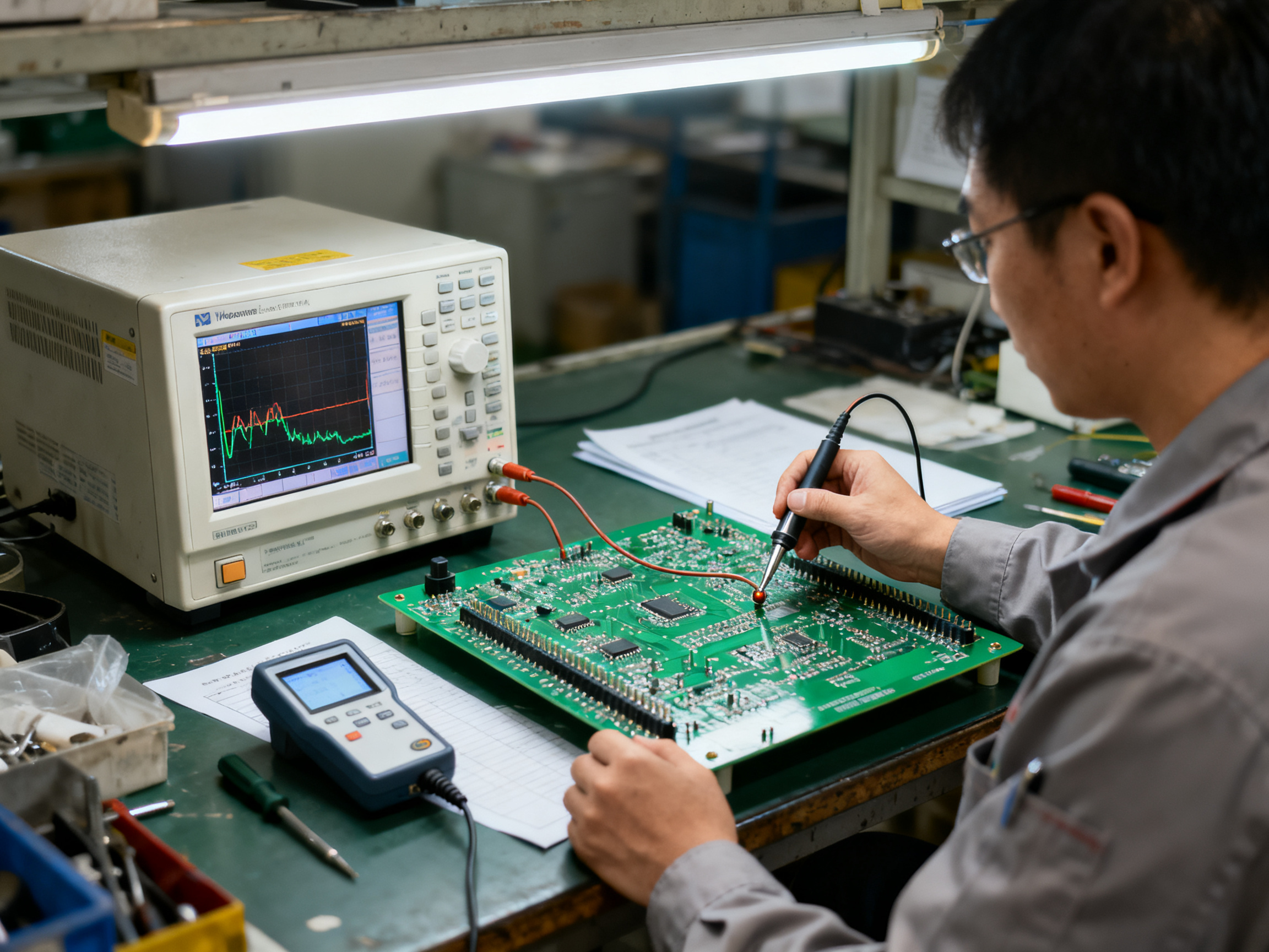
| Parameter | Lead-Free (SAC305) Target | Notes |
|———–|————————–|——-|
| Solder pot temperature | 255-265°C | Higher than tin-lead due to SAC liquidus |
| Topside preheat | 120-150°C | Depends on board thickness and copper density |
| Preheat-to-wave delta | Below 150°C | Prevents thermal shock to components |
| Conveyor speed | 1.0-1.4 m/min | Slower than tin-lead for adequate contact time |
| Wave contact time | 3-5 seconds | Per IPC J-STD-001 Rev H (2026) |
| Wave height | 0.5-0.67 of board thickness | Adjust based on defect patterns |
| Cooling zone exit temp | 100-120°C topside | Balances grain structure and thermal stress |
| Bath copper check | Every 8,000 boards | Keep below 1.0% for SACX alloys |
The market data tells us wave soldering isn’t going anywhere. Projections show the wave soldering equipment market growing from $1.8 billion in 2025 to $3.1 billion by 2034. That’s real momentum behind a technology that still delivers the best throughput for high-volume through-hole production.
If you’re running wave soldering in your facility, you’ve got the foundation. Now it’s about tightening your process, building your documentation, and running lines that your customers trust to deliver quality, board after board.
Now that you understand the wave soldering process flow inside and out, you’re ready to take your production quality to the next level.