
Published: October 30, 2026
Last Updated: October 30, 2026
Reading Time: 25 minutes
Written by: [Author name and relevant credentials]
Reviewed by: [Qualified reviewer name and credentials, if assigned]
Note to editors: the author and reviewer fields above are intentional placeholders. Do not publish this guide until verified names, roles, and SMT credentials are supplied for both lines.## Choosing the Right Soldering Process
The right soldering process depends less on whether a board is “SMT” than on its component mix, throughput, acceptable defect rates, and how much rework the production model can absorb.
Reflow Soldering
Reflow is the default for most surface-mount assemblies. Solder paste is printed onto the PCB pads, components are placed, and the entire assembly passes through a controlled heating cycle. The solder melts, wets the component terminals and copper lands, and solidifies as the board cools.
Use reflow when the board contains predominantly leadless surface-mount components, especially fine-pitch devices, BGAs, QFNs, and dense two-sided assemblies. It applies controlled heat to all joints at once, so there is less opportunity for uneven heating than with individual hand or wave soldering.
A typical lead-free profile uses a rapid ramp from ambient temperature to soak, a soak period that activates the flux, a controlled rise to peak temperature, and a sufficiently long cooling phase. The exact temperatures depend on the solder alloy, paste, component packages, and board construction. SAC305 is commonly processed around a 235–245 °C peak, while SAC305-compatible paste specifications may establish a narrower or slightly different working range.
For conventional Sn63/Pb37, peak temperatures are commonly around 215–225 °C. Mixed-alloy boards require special care because the melting behavior of the resulting solder can create uncertain solidification temperatures.
Wave Soldering
Wave soldering remains useful for through-hole and mixed-technology assemblies. A pump creates a wave of molten solder, and the board is moved through the wave so that solder enters plated through-holes and wets the exposed component leads. Thermal mass, preheating, flux application, wave height, speed, and cooling must be coordinated to prevent bridging, insufficient filling, or damage.
Wave soldering is generally less suitable for leadless fine-pitch packages because the board must be exposed to a broad thermal cycle and extensive handling. Its strongest application is a board dominated by through-hole connectors, transformers, capacitors, and similar components.
Selective Soldering
Selective soldering applies heat locally with a soldering iron or a controlled nozzle, usually beneath a stencil or fixture. It offers more precise thermal control than conventional wave soldering and is often used on mixed-technology boards where only designated areas may contact molten solder.
Selective soldering can reduce solder exposure for heat-sensitive or mechanically sensitive components, but it does not automatically solve process problems. Flux residue, tip temperature, contact time, nozzle geometry, and board positioning still determine joint quality. The method is best treated as a controlled production process rather than as a faster substitute for wave soldering.
Pin-in-Paste
Pin-in-paste, or wave-soldering alternatives that preform solder on component leads, can simplify some through-hole and mixed assemblies. Solder is applied to selected leads before the board enters the wave. The wave then completes wetting and reflow at those joints.
This approach can reduce the wave contact time and limit solder exposure to areas that do not require it. However, it adds pre-forming equipment and process steps. It is most compelling for high-volume mixed-technology products rather than low-volume prototypes.
Hand Soldering and Drag Soldering
Hand soldering is appropriate for prototypes, repair, rework, and low-volume assembly. A temperature-controlled iron should normally be used with a suitable tip shape and a flux-bearing solder wire. The iron heats the joint; the solder wire supplies the alloy. Holding the wire against the iron and heating both together can produce an oxidized, poorly wetted joint.
Drag soldering uses molten solder dragged across a row of joints to solder multiple pins simultaneously. It can be efficient for leaded packages, but it is difficult to control on fine-pitch leadless devices. Excessive drag time can heat the package beyond its rating, while insufficient dwell can produce poor wetting.
Practical rule: Choose the process based on the most demanding component and the required production volume. A board containing a fine-pitch BGA should generally start with reflow, even if many of its other parts would be easier to solder by hand.
Essential SMT Tools and Equipment
A capable SMT line usually includes several distinct systems. Each performs one tightly controlled operation.
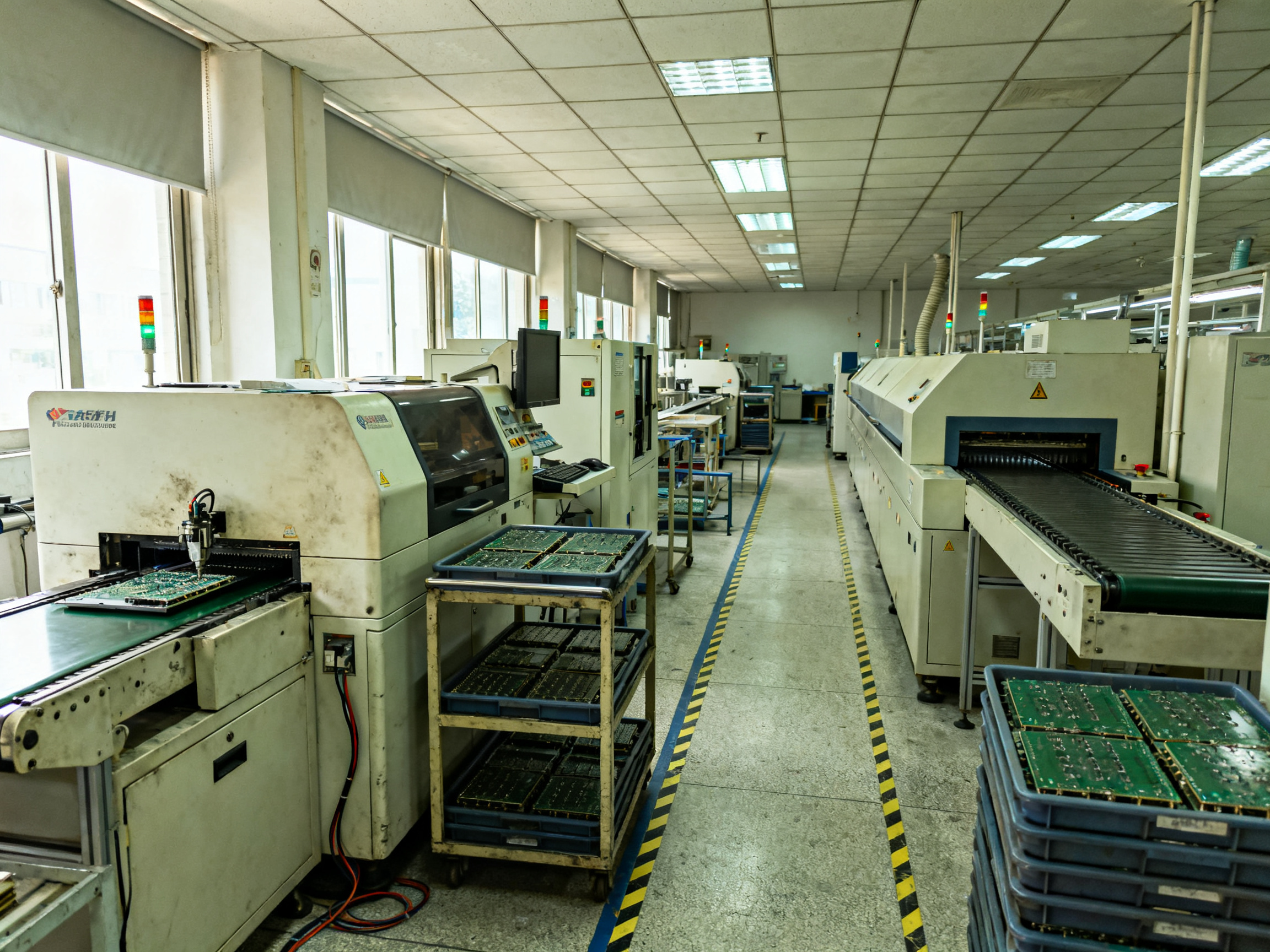
Solder Paste and Storage
Use paste specified for the alloy, component termination finish, and assembly process. Store lead-free paste according to the supplier’s instructions, typically in a refrigerated cabinet when required, and allow it to reach the appropriate temperature before opening. Condensation or repeated temperature cycling can damage paste consistency and printing performance.
For prototype work, a small jar may be sufficient. Production lines generally need automated dispensing or bulk feeding, paste-temperature monitoring, and a defined inspection interval for the stored material.
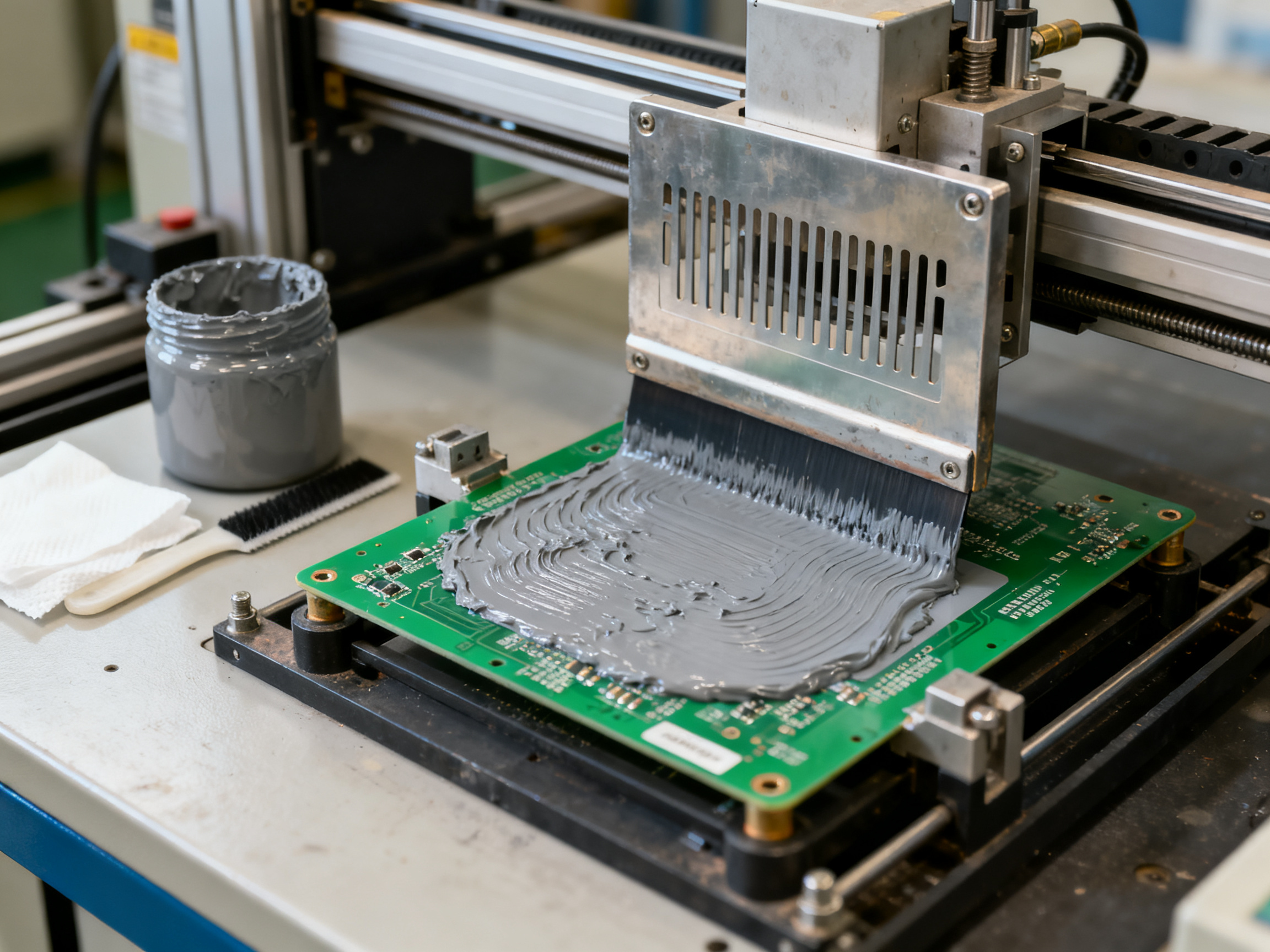
Stencil Printer and Stencil
The stencil deposits a controlled amount of paste on each land. A properly etched laser or electroformed stencil improves paste release, but print parameters matter just as much. Check squeegee condition, blade pressure, separation speed, aperture alignment, substrate cleanliness, and paste condition before troubleshooting the reflow profile.
Fine-pitch apertures are particularly sensitive to the ratio of aperture width to paste thickness. Printing too thick can increase bridging risk, while printing too thin can reduce solder volume. The correct target depends on the component pitch, pad geometry, paste solid content, and manufacturer recommendations.
Pick-and-Place System
The placement system must handle the component’s dimensions, package type, and orientation accurately. Feeder setup errors, wrong tape positions, incorrect nozzle selection, and vision misreads can all mimic soldering defects.
Before reflow, inspect placement carefully:
- Confirm that each component matches the bill of materials.
- Check polarity marks, diodes, electrolytic capacitors, and IC orientations.
- Verify that components are seated evenly rather than tilted on one side.
- Inspect staggered or fine-pitch terminals for shifted or partially lifted parts.
Reflow Oven
A useful reflow oven must control ramp rates, soak time, peak temperature, time above liquidus, and cooling. It should also provide profile logging and repeatable loading behavior. Conveyor speed alone does not define the thermal profile; the actual board temperature over time is what matters.
When comparing ovens, evaluate:
- Temperature stability and repeatability across the working zone.
- Profile logging and data export.
- Airflow or conduction uniformity.
- Thermal mass handling.
- Support for the package and board sizes used in production.
- Ease of process qualification, maintenance, and calibration.
A precise temperature display at one point in the chamber is not enough. The useful question is whether the assembly sees the specified profile consistently from one run to the next.
Inspection and Measurement
Visual inspection remains important, but the defect types associated with hidden joints require additional tools. X-ray inspection reveals solder volume, voids, bridging, and missing connections beneath BGAs and QFNs. A scanning acoustic microscope can detect delamination or other internal interface defects. Electrical testing verifies functional connectivity but does not explain why a joint failed.
Common production instruments include:
- Laser profilometers for paste-inspection measurements.
- SPI systems for solder-paste volume, area, height, and alignment.
- AOI systems for polarity, placement, missing components, solder appearance, and some bridge detection.
- X-ray systems for hidden terminations and package interiors.
- Scope-based solderability or wetting assessments during process qualification.
A Defensible Reflow Temperature Framework
A solder alloy’s nominal melting range is not a complete reflow recipe. The assembly process must satisfy both the solder supplier’s recommendations and component manufacturers’ ratings.
Lead-Free SAC Alloys
SAC305, a commonly used tin-silver-copper alloy, has a nominal melting range near 217–220 °C. Its peak reflow temperature is commonly around 235–245 °C, depending on the paste formulation and package constraints. The time above liquidus must be long enough to form reliable joints without unnecessarily stressing the assembly.
Do not copy a universal peak temperature across every board. Consider:
- Paste supplier limits.
- Component maximum reflow temperatures and package classifications.
- PCB laminate temperature ratings.
- Oven uniformity and calibration.
- Board size, component density, and thermal mass.
- Whether the assembly contains temperature-sensitive components.
Tin-Lead Alloys
Sn63/Pb37 has a nominal melting point near 183 °C and is often processed with a peak around 215–225 °C. The lower alloy temperature can reduce thermal stress, but lead-containing processes carry occupational, waste-disposal, and legal obligations that must be assessed for the manufacturing location and market.
What “Too Hot” Means
A peak temperature that exceeds a component’s rating can damage packages, passivations, die attachments, or internal bonds. It can also accelerate intermetallic formation and embrittlement. Conversely, a profile with insufficient peak temperature or time above liquidus can cause incomplete melting, poor wetting, and weak or dull joints.
For qualification, record the profile on the board rather than relying only on the oven’s set points. Place thermocouples near the smallest components, on thermally representative locations, and avoid attaching them directly to delicate leads where the attachment itself could distort the result.
Step-by-Step SMT Assembly
A repeatable SMT assembly process follows the same basic sequence each time.
1. Verify the Materials
Confirm the PCB revision, component list, solder alloy, paste type, stencil revision, and placement data. Inspect the boards for contamination, scratches, oxidation, warpage, and damaged pads. Surface cleanliness is essential because contaminants can prevent solder wetting and flux removal.
2. Print the Solder Paste
Load the paste into the printer and verify the correct stencil orientation and alignment marks. Run a few test prints and inspect them under magnification or with SPI. Check paste coverage, alignment, uniformity, and volume before starting a production run.
A commonly cited process target is paste transfer efficiency above 70%, although the appropriate threshold depends on aperture geometry and the supplier or industry process requirement. The important principle is consistent transfer onto the intended lands without excessive material on adjacent apertures.
3. Inspect the Print
Look for:
- Missing or insufficient paste.
- Paste deposited between fine-pitch apertures.
- Smearing caused by poor stencil release.
- Uneven paste thickness.
- Misalignment between stencil apertures and PCB lands.
- Foreign material or dried paste fragments.
Correct paste problems before placement. A blocked or damaged aperture cannot be repaired reliably by changing the reflow temperature.
4. Place the Components
Load each feeder and verify its orientation against the placement file. Run the placement system in a dry-run or placement-verification mode when practical. Confirm that the board origin, rotation, and component coordinates match the CAD data.
After placement, inspect the board for missing parts, reversed parts, shifts, incorrect polarity, and components sitting on or beyond their pads. A small amount of component misalignment can still be acceptable for a robust leaded package while remaining catastrophic for a fine-pitch leadless device, so package-specific criteria are necessary.
5. Reflow the Assembly
Confirm the oven recipe and material set before loading the board. Profile the actual assembly if the recipe is new or the oven, board, or component mix has changed. During the cycle, observe the solder’s melting behavior for gross anomalies such as premature activity, insufficient wetting, or excessive smoking, but do not judge final quality until the board has cooled and has been inspected.
6. Cool and Clean
Allow the board to cool naturally within the process specifications. Forced cooling can improve cycle time but must be controlled so that it does not create thermal shock or uneven solidification. Remove flux residue only with a cleaning process validated for the flux chemistry, board materials, components, and downstream requirements.
7. Inspect and Test
Perform visual or AOI inspection before handling the board aggressively. Use X-ray inspection for hidden joints when required, and use in-process or functional electrical testing to verify the assembly. Keep inspection criteria consistent; changing what counts as acceptable between operators creates false yield data and obscures process trends.
8. Document the Run
Record the paste lot, print settings, placement program version, oven recipe, profile data, inspection results, and any deviations. Reliable production data turns troubleshooting from guesswork into a controlled improvement process.
Diagnosing Common Soldering Defects
A defect is usually a symptom of several interacting conditions. Correcting only one visible symptom can hide the underlying process weakness.
Cold or Poorly Wetted Joints
Appearance: The joint may be dull, grainy, irregular, or insufficiently fused.
Common causes:
- Insufficient reflow temperature or time above liquidus.
- Excessive ramp rate.
- Degraded or improperly stored paste.
- Poor flux activity.
- Contaminated pads or terminations.
- Inadequate solder volume.
- Incorrect alloy for the component or process.
Corrective actions:
Verify the board profile, paste condition, stencil deposit, and pad cleanliness. Do not increase oven temperature without confirming the component rating and the actual temperature experienced by the assembly.
Solder Bridging
Appearance: Solder connects adjacent pads or terminals that should remain separate.
Common causes:
- Excessive paste volume.
- Poor stencil release.
- A damaged or blocked aperture.
- Incorrect pad design.
- Placement error.
- Excessive solder during manual rework.
Corrective actions:
Inspect the paste print first, then review pad geometry and placement accuracy. Reflow alone will not cure excessive or misplaced solder volume.
Tombstoning
Appearance: A small chip capacitor stands vertically on one termination, or one end lifts away from the pad during heating.
Common causes:
- Uneven paste deposits.
- Poor pad design or thermal balance.
- Excessive heating rate.
- Solderability issues on one termination.
- Incorrect paste volume.
Corrective actions:
Improve print consistency, review the PCB pad geometry, and qualify a suitable ramp rate. Confirm that the component terminations have reliable solder coating.
Insufficient Solder on BGA Joints
Appearance: X-ray shows a missing ball connection, a small joint footprint, or inadequate solder volume.
Common causes:
- Lost or displaced solder during handling.
- Insufficient paste deposition or transfer.
- Component movement before reflow.
- Incorrect stencil thickness or aperture design.
- Excessive voiding.
- Board or component warpage.
- Inadequate reflow.
Corrective actions:
Examine the X-ray image quantitatively rather than relying only on a general visual impression. Review print results, placement stability, board support, paste volume, and the reflow profile.
Voiding
Appearance: Gas or flux-related cavities form within the solder joint.
Common causes:
- Excessive outgassing from the PCB or component.
- Flux decomposition characteristics.
- Insufficient time above liquidus.
- Poor venting in the component package.
- High moisture or contamination.
Corrective actions:
Use a voiding-controlled paste where appropriate, verify drying and cleaning procedures, and confirm sufficient reflow dwell. Excessive liquidus time is not a universal cure because it can increase intermetallic growth and damage packages.
QFN Corner Separation
Appearance: Solder does not reach part of the exposed pad perimeter or leaves a gap at a corner.
Common causes:
- Insufficient paste volume.
- Uneven thermal loading.
- Poor pad design.
- Wicking to the ground pad without adequate wetting of the perimeter.
- Incorrect stencil thickness.
Corrective actions:
Review paste volume and aperture design, inspect the thermal pads for contamination, and confirm that the reflow profile provides sufficient wetting time. X-ray inspection is important because the defect may be hidden beneath the package.
Head Wetting and Insufficient Joint Formation
Appearance: Solder wets the vertical component lead but retreats from the pad, or the fillet appears sharp and unbalanced.
Common causes:
- Poor pad geometry.
- Inadequate paste deposit.
- Excessive heating of the component lead relative to the pad.
- Oxidation or contamination.
- Incorrect board finish.
Corrective actions:
Check paste volume, board finish, and pad design. For rework, use controlled heat distribution rather than holding the iron on one side of the joint.
Practical Rework Guidance
Rework requires more care than assembly because the board and component have already experienced one thermal cycle. Protect nearby parts with an approved heat shield, use a controlled hot-air or rework station, and keep the airflow away from adjacent components. Select the nozzle for the package footprint and keep the rework profile within the component manufacturer’s limits.
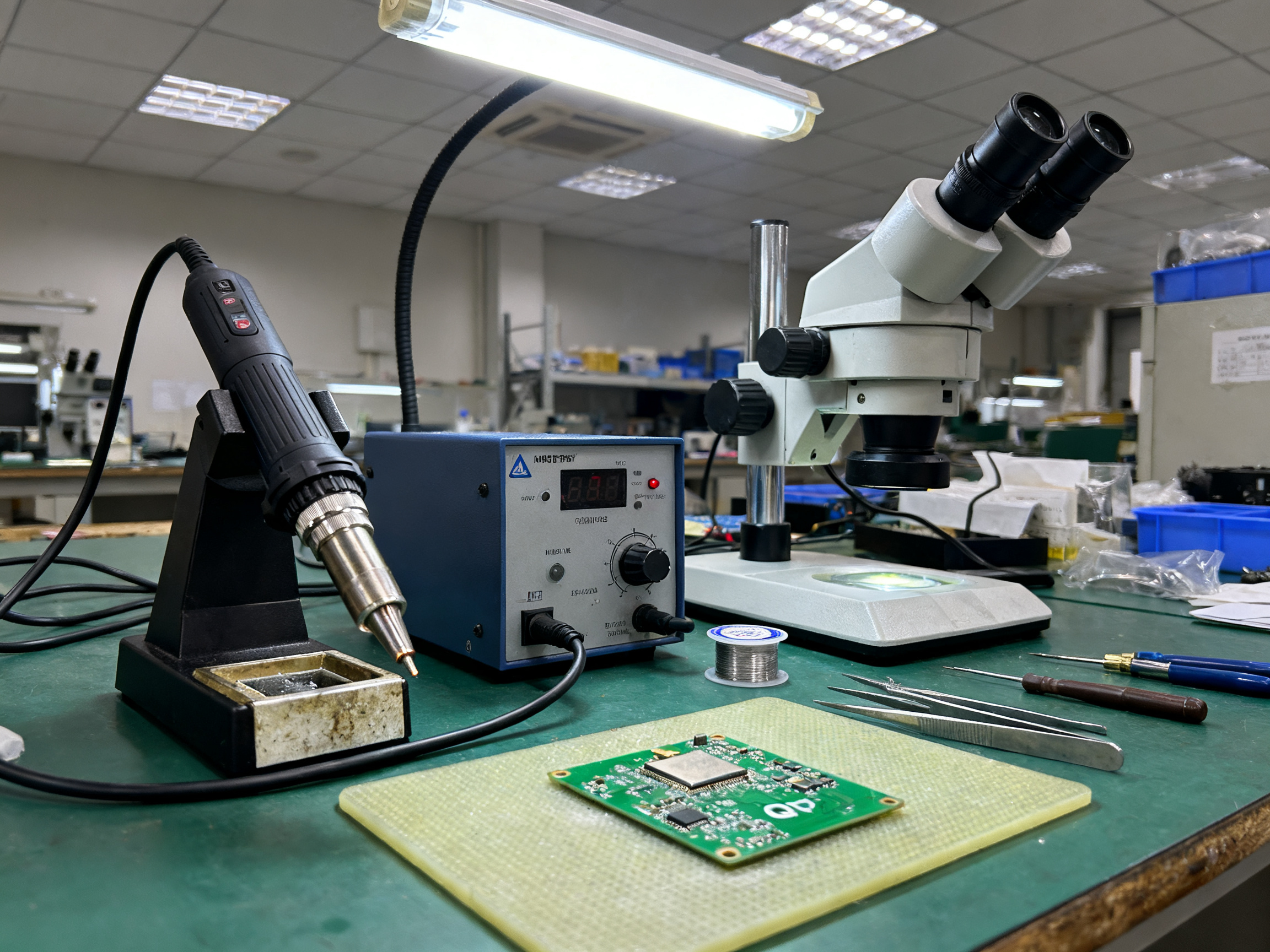
For BGA removal, use a controlled heating profile with adequate soak and ramp control. Remove the package while the solder remains molten, clean the lands, inspect them under magnification, and apply fresh paste or a controlled volume of solder before replacement. A full-board replacement may be more reliable than repeated site-level heating if several joints are already degraded.
For QFN rework, divide the process into pad preparation, component removal, pad cleaning, solder or paste application, and placement. Check the exposed pad for coplanarity after reflow. Excessive solder under the package can create an unstable assembly, but too little solder leaves the component unsupported.
Avoid reheating a joint repeatedly. Each cycle can thin the solder through evaporation, increase intermetallic layers, and raise the risk of pad or trace failure. If a rework operation fails, stop and inspect the board before trying again.
Building Reliable SMT Production
The strongest SMT process is not the one with the most sophisticated equipment; it is the one whose variables are understood and controlled. Begin with the component package and paste volume, not the oven setting. Confirm that the board receives appropriate solder, then verify that it receives heat for the required time. Finally, inspect the result and preserve the data.
Scale gradually by qualifying the materials, print settings, placement program, thermal profile, inspection criteria, and cleaning process. Use control charts to monitor paste volume, placement accuracy, defects, and first-pass yield. When a defect rate rises, determine whether the shift originated in printing, placement, reflow, handling, or inspection before changing the recipe.
That discipline becomes more important as boards become denser. Smaller packages and tighter pitches reduce the process margin, and a defect that was harmless on a through-hole assembly can make a leadless component unmanufacturable. Reflow remains the central process for modern SMT, but reliable production depends on the entire chain around it.## About the Author
Placeholder section. Do not publish until the fields below are completed and verified by the publisher.
[Author name] is [verified role or credential] with experience in [verified SMT, electronics manufacturing, process engineering, or technical procurement area]. [He/She/They] has contributed to [verified relevant project, application, or achievement], which informs the practical guidance in this article.
No author name or biography was supplied when this guide was written, so we have left the brackets in place rather than inventing credentials. That matters here. This article covers reflow profiles, tip temperatures, inspection criteria, and equipment choices, and readers may act on what they read. An anonymous author on a technical buying guide helps nobody.
Once verified details are provided, this section will list the author’s real role and hands-on work, and a reviewer line will confirm the SMT qualifications behind the technical review. Reviewers should check the temperature windows, defect causes, and acceptance criteria against current IPC and JEDEC documents before sign-off.
Editors: replace the bracketed text with verified credentials only. Do not paraphrase or soften unverified claims.## 2. The SMT Production Line: From Solder Paste to Inspection
A modern SMT line is a sequence of controlled steps. Each stage prepares the board for the next one, and small defects can become expensive if they are allowed to continue. The goal is not simply to place components on a PCB; it is to create repeatable, inspectable solder joints while protecting sensitive packages from heat and contamination.
The basic process
- PCB preparation — The bare board is cleaned and inspected for defects, contamination, oxidation, and proper pad patterns.
- Solder paste printing — A stencil applies a controlled layer of solder paste to the PCB pads. The stencil aperture, paste volume, and board registration directly affect the amount of solder deposited.
- Component placement — Pick-and-place machines identify each component from its packaging, rotate it as needed, and place it onto the paste-covered pads.
- Reflow soldering — The board passes through a reflow oven or is heated with an equivalent controlled profile. Solder paste melts, wets the component terminals and copper pads, and forms the electrical and mechanical connection.
- Cooling — The board cools in a controlled manner so the solder joints solidify without excessive thermal shock or movement.
- Inspection — Operators and automated systems check placement, solder joints, polarity, and other assembly requirements.
- Testing and finishing — Electrical tests, conformal coating, depanelization, and final packaging may follow depending on the product.
The important idea is that paste printing and component placement happen before reflow. Reflow does not move components into position; it transforms the printed paste into finished solder joints.
Solder paste printing
The stencil is a thin metal or laser-cut sheet with openings aligned to the PCB pads. During printing, the machine presses solder paste through those openings and then uses a wiper blade to remove excess material. The result should be a small, consistent deposit on each pad—not a spreading blob that can shift the component.
A common defect is insufficient paste. If there is too little solder, the joint may not reach full electrical contact. Excessive paste can create bridging between adjacent pads, especially on fine-pitch ICs. The correct result depends on the package geometry, pad design, and paste type.
Solder paste also contains flux and other chemicals that help the solder wet the surfaces during heating. Because the paste remains on the board during reflow, its formulation must match the component finish and the assembly process. Printing and storage conditions matter too: paste exposed to air can absorb moisture or develop a poor working consistency.
Pick-and-place
The placement machine receives a bill of materials, also called a BOM, and a list of board coordinates. The BOM identifies the part, while the coordinate file tells the machine where each part belongs on the PCB. Together they tell the machine what to place and where.
Modern machines can place components as small as 0201 packages and handle boards containing thousands of parts. They use vision, feeders, calibration marks, and sometimes component inspection to confirm placement orientation and position.
Placement accuracy is especially important for leadless packages. A QFN or QFP can appear to be correctly aligned while still having a terminal positioned incorrectly over its pad. Reflow will then pull that terminal toward the nearest solder deposit, producing a short, an open connection, or a noncompliant joint.
Reflow soldering
Reflow soldering uses a controlled temperature profile to bring the solder to its melting point and then cool it properly. A typical profile has several phases:
- Preheat — The board and components warm gradually, reducing the temperature difference between them.
- Soak or liquid phase — The solder paste reaches a liquid state and activates the flux.
- Peak or reflow phase — The solder reaches its target temperature and forms the joint.
- Cooling — The board cools while the solder solidifies.
The profile is not a single temperature setting. It is a time-versus-temperature curve, and the correct curve depends on the solder paste, component packages, PCB materials, board construction, and thermal mass. A board with large copper areas may need a different profile from one with small, densely populated areas.
Reflow is also where component limits matter. Large packages, connectors, and heat-sensitive parts may require careful profiling. The oven should provide enough airflow and temperature control to create repeatable results across the entire board, not just at its center.
AOI and X-ray inspection
Automatic optical inspection, or AOI, is commonly used after reflow to check visible solder joints and component placement. It is effective for polarity marks, missing components, skewed parts, bridges, and many through-hole or visible-terminal defects.
AOI cannot see every joint. Solder underneath a component, inside a QFN, or beneath a BGA may be hidden from the camera. For those packages, X-ray inspection is often used. X-ray systems reveal solder volume, voids, bridging, and missing connections without looking at the board’s visible surface.
Inspection should be treated as a process-control tool, not just a pass-or-fail gate. When a defect pattern appears, the line should investigate what caused it: paste volume, stencil condition, placement accuracy, reflow profile, component quality, or board handling.
Why process order matters
The order of operations is deliberate. Printing before placement allows paste to act as a temporary adhesive that holds parts during reflow. Inspection after reflow confirms whether the thermal process produced acceptable joints. If through-hole parts are added later, their soldering must not damage the surface-mount assembly.
In a mixed-technology line, surface-mount components are generally assembled first. Through-hole components may then be inserted and wave soldered, selectively soldered, or hand soldered. The sequence is chosen around component heat tolerance, accessibility, and the risk of rework.
Practical rule: A good SMT line is not defined by the speed of one machine. It is defined by whether every step is repeatable, measurable, and controlled.
The next section looks at the tools and materials used at the bench, including soldering irons, hot-air rework stations, flux, solder wire, and the question of when each method is appropriate.## 2. How the SMT Soldering Process Works from Paste to Inspection
A reflow joint is made in under four minutes. The decisions that determine whether it works were made long before the oven started.
The SMT soldering process runs as a chain of controlled steps, and every step hands something to the next one. When a defect shows up at final test, the cause is usually two or three stations upstream.
The flow
PCB Prep → Paste Print → SPI → Placement → Reflow → Cooling → AOI/X-ray → Electrical Test → Rework or Ship
Here is what each station actually controls:
- PCB preparation. Clean and inspect for contamination, oxidation, scratches, warpage, and pad damage. A fingerprint on a fine-pitch land can turn into a dry joint later.
- Stencil printing. A thin metal or laser-cut stencil deposits a controlled amount of solder paste onto the lands. Aperture design, paste volume, blade pressure, separation speed, and board registration all matter here.
- Solder paste inspection. SPI checks height, area, volume, and alignment before anything is placed. This is your earliest pad-level evidence. iNEMI’s SMT printing roadmap points to stable transfer efficiency above 70% for small apertures as a key industry need for reference.
- Component placement. The pick-and-place machine uses a BOM for identity and a coordinate file for location. Vision, feeders, and calibration confirm orientation and position.
- Reflow. The board passes through a controlled heating curve. Flux activates, solder melts, wets the terminals and lands, and a thin intermetallic layer forms between the alloy and the copper.
- Cooling. Solidification happens here, and it is where grain structure and joint strength are set. Forced cooling can save cycle time but has to be controlled so it does not create thermal shock or uneven shrinkage.
- Inspection. AOI handles visible joints, polarity, missing parts, and skew. X-ray handles what cameras cannot see, which means BGA balls, QFN voids, and hidden bridges.
- Testing. Functional or in-process electrical tests confirm connectivity. They confirm that a joint works, but they rarely tell you why it failed.
Pro Insight: On one line we reviewed, a recurring batch of “cold joint” rejects on a two-row connector turned out to be a stencil issue, not a reflow issue. The reflow profile was correct and the oven was calibrated. SPI had flagged only one aperture in the stencil as under-filled, and a stuck fragment of dried paste was sitting in that aperture. The fix was cleaning the stencil and adding a wipe-down step to the changeover. The measurement that cracked it was the SPI volume data, not the oven chart. Had the team raised the peak temperature, they would have damaged good components and still shipped bad joints.
Critical control points
| Stage | Key variable | How to measure | Likely defect |
| — | — | — | — |
| Paste printing | Volume, height, alignment, transfer efficiency | 3D SPI, print weight check | Insufficient solder, bridging, solder balls |
| Placement | Offset, rotation, seating | Placement verification, AOI | Opens, shorts, tombstoning, skewed parts |
| Reflow | Peak temp, ramp rate, time above liquidus | Thermocouple profile on the actual board | Cold joints, insufficient wetting, voiding |
| Cooling | Cooling rate, uniformity | Profile data, solder appearance | Cracking, non-uniform grain, thermal shock |
| Inspection | Criteria stability, false-call rate | Gage R&R, review records | Escaped defects, wasted real estate on false calls |
How the machines talk to each other
Conveyors and line protocols are the plumbing that holds the sequence together. IPC-HERMES-9852 handles board transport and identity between adjacent machines, and IPC-2591 CFX covers two-way factory data exchange with host software. Both are voluntary unless a contract invokes them, but they are how traceability data from a machine ends up attached to a finished board.
The same applies to standards such as IPC J-STD-001 and IPC-A-610, which cover soldering and workmanship acceptance. They become binding only when a contract, drawing, or customer quality plan says so. If you are new to how to do SMT soldering properly, start with the idea that each station produces records. Paste lot, print settings, placement program version, recipe, profile data, inspection results, and any deviation belong in the same trail.
Why line order matters
Printing happens before placement because the paste acts as a temporary adhesive. If you place components first, you need glue, and glue outgasses, which creates voids.
In mixed-technology builds, surface-mount parts usually go first. Through-hole parts then get inserted and wave soldered, selectively soldered, or hand soldered. That order is chosen around heat tolerance and access, not convenience.
Practical rule: If you want to know how to do SMT soldering with less rework, instrument the earliest station where the symptom is visible. SPI tells you about solder. AOI tells you about placement. X-ray tells you about hidden joints. Thermal profiling tells you about heat. Each tool answers a different question.
For lines running consumer electronics, semiconductor, or military work, the reflow oven and wave soldering equipment from S&M Co. Ltd. (Shenzhen Chuxin Electronic Equipment Co., Ltd.) are built for high-density assemblies where defect reduction on BGA and QFN parts is the main worry. Machines that suit your board sizes and connect to standard line protocols are worth comparing against any incumbent setup.## 3. SMT Soldering Tools and Equipment: Bench Setup to Full Production Line
Tools make the difference between a joint you can repeat and a joint you got lucky with. But you do not need a full line to start, and you should not buy a full line before you know what the work actually demands.
The cleanest way to think about it is three tiers.
Essential (bench and repair)
- Temperature-controlled soldering iron. Never an unregulated mains iron. A station with a digital readout and adjustable wattage gives you a repeatable starting point.
- Tip assortment. Chisel and bevel tips move heat better than needle tips. Match the tip to the joint and the pad.
- Hot-air rework station. Needed for QFN, BGA, and leadless rework where an iron alone will not work.
- Stereo microscope or loupe. Eyewear helps. A 10x loupe costs little and changes everything on an 0402 joint.
- Tweezers, brass wool, solder wick, flux.
- Solder wire matched to your alloy choice, ideally with a no-clean or halide-free flux core.
- Pad cleaning. Isopropyl alcohol and a lint-free wipe. Contamination causes more failures than bad soldering does.
Recommended (process control)
- Preheater. Lifts the whole board before you touch a joint, which cuts dwell time and protects large thermal masses.
- Tip thermometer. Station setpoint is not working-tip temperature. Hakko’s guidance on verifying iron tip temperature recommends a calibrated instrument and repeated stabilized readings on a clean, tinned tip, because the number on the panel drifts from the real face temperature reference.
- Fume extraction. Capture at the source, not across the room. Flux fumes and lead dust carry real exposure obligations under OSHA guidance.
- Documented ESD program. Grounded bench, controlled flooring, wrist straps with periodic testing, and training. A wrist strap on its own is not a program.
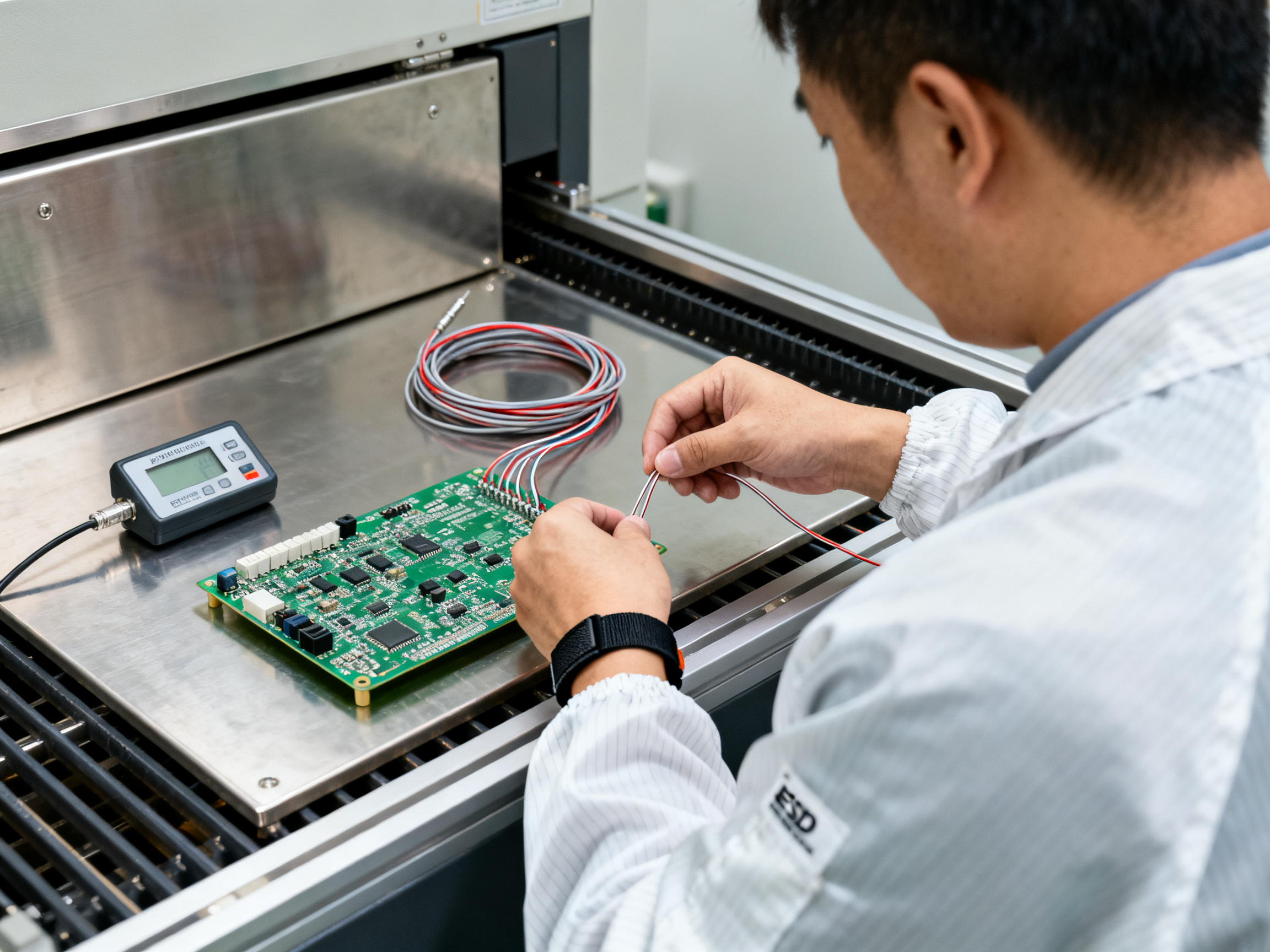
Production scale
Stencil printer, SPI, pick-and-place, reflow oven, AOI, X-ray, wave or selective soldering, and the conveyors and data links that hold them together.
From Our Experience: The most telling difference between a hobby bench and a working production area is not the iron or the microscope. It is the documentation habit. Lines that record tip temperature checks, paste lot numbers, placement program versions, and profile data can answer “why did this board fail” in minutes. Lines that do not are stuck guessing, and guessing gets expensive fast.
Comparing the heat sources
| Method | Best for | Watch out for |
| — | — | — |
| Soldering iron | Prototypes, repair, leaded joints | Tip temperature droop on heavy copper, one joint at a time |
| Hot air rework | QFN, BGA, leadless removal | Airflow damages neighbours, needs preheat and control |
| Reflow oven | Leadless and fine-pitch production | Profile must match the actual populated board |
| Wave soldering | Through-hole and mixed assemblies | Dross, bridging, thermal load on the board |
| Selective soldering | Localised through-hole joints among SMD | Nozzle geometry and board positioning |
Process infrastructure people forget
Consumables storage with temperature control, calibration schedules for tip thermometers and inspection equipment, nitrogen capability where your alloy and package mix demand it, and maintenance plans for preheaters, wave pots, and stencil printers. All of it affects cost per accepted board, not just purchase price.
Practical rule: Buy the tool that answers the question you are failing to answer. If you cannot see the joint, add inspection. If you cannot repeat the heat, add profiling. If you cannot control the environment, fix the environment first.
For high-density work in consumer electronics, semiconductors, or military programs, the lead-free reflow ovens and wave soldering machines built by S&M Co. Ltd. (Shenzhen Chuxin Electronic Equipment Co., Ltd.) target BGA and QFN defect reduction and fit standard line protocols, which is worth comparing against whatever you are running now.## 4. Reflow Soldering Step by Step: Paste, Placement, and Thermal Profiling
Reflow is where the whole SMT soldering process cashes out. You can print perfectly, place perfectly, and still destroy the board with a bad thermal cycle. The good news is that the recipe is measurable. You do not have to guess.
The sequence, in order
- Stencil alignment. Register the stencil to the PCB using the alignment marks, then run a wipe cycle and a test print. Check the deposit under magnification before you commit to a run.
- Paste deposition. The blade pushes paste through the apertures, and the stencil lifts away. Squeegee condition, blade pressure, separation speed, and paste condition all change the volume.
- Component placement. The pick-and-place machine sets parts onto the paste, which holds them like glue until the heat arrives.
- Thermal profiling. You measure the real board, then set the recipe to match.
- Reflow cycle. Preheat, soak, peak, cool.
- Cooling. Solder solidifies here. Rush it and you get grain problems.
- Post-reflow inspection. AOI for what a camera can see, X-ray for what it cannot.
The thermal profile, broken into phases
   Temp (°C)
   260 ┤
       │              ╭─╮  PEAK (230-250 °C lead-free)
   240 ┤            ╭─╯╰─╮
       │          ╭─╯    ╰────╮
   220 ┤        ╭─╯            ╰─   ← liquidus ~217-220 °C (SAC305)
       │      ╭─╯                 ╰╮
   180 ┤    ╭─╯  SOAK (140-160 °C)  ╰╮
       │  ╭─╯                        ╰╮
   150 ┤╭─╯                            ╰╮
       ││                                 ╲
    25 ┼┴──────────────────────────────────╴──► Time
        PREHEAT   SOAK    PEAK   COOL
- Preheat brings the board up gradually. Aim for roughly 1.0 to 1.5 °C per second. A fast ramp shocks big components and skews tiny ones.
- Soak at about 140 to 160 °C gives the flux time to activate and the board to even out. Roughly 20 to 60 seconds is common.
- Time above liquidus is where the joint actually forms. Around 217 °C and above for 45 to 60 seconds is a common working window for SAC pastes.
- Peak usually lands near 230 to 260 °C for lead-free work. AIM puts SAC305 melting around 217 to 220 °C with a typical peak window of 240 to 250 °C reference.
- Cooling at roughly 2 to 6 °C per second gives a dense joint without thermal shock.
Those numbers are starting points, not commandments. The actual window comes from your paste datasheet, your component ratings, your board mass, and the temperature your product actually sees.
Expert Tip: Profile the actual populated board, every time you change something. Do not copy a setpoint recipe from a different product and hope. Attach thermocouples to a real, loaded assembly near the smallest and the largest components, run the cycle, and read the curve. A board with a big copper ground pour on one side and a tiny 0402 cluster on the other will never follow a copied recipe. We have seen a “proven” profile produce dry joints on one product and cracked packages on another, simply because both were run on the same recipe with no board-level measurement.
Pre-reflow checklist
| Check | Why it matters |
| — | — |
| Paste lot, alloy, and storage condition | Degraded paste prints poorly and wets poorly |
| Stencil revision and aperture condition | A blocked aperture starves the joint |
| Board cleanliness and pad condition | Contamination blocks wetting |
| Component placement verified, polarity checked | Reflow will not fix a reversed part |
| Oven calibrated, recipe loaded and confirmed | Setpoints drift, especially with nitrogen |
| Board support and panelisation | Warpage drives voids and head-in-pillow |
| Atmosphere decided | Air or nitrogen changes oxidation and drying behaviour |
Defect, cause, correction
| Defect | What it looks like | Most likely cause | What to change |
| — | — | — | — |
| Tombstoning | Chip part standing on one end | Uneven paste volume, too fast a ramp, poor pad balance | Fix print consistency, slow the ramp, review pad design |
| Head-in-pillow | Joint formed on one side only | Component moved during soak, poor paste volume | Check placement stability and paste volume, extend soak control |
| Voids | Cavities inside the joint | Outgassing, short time above liquidus | Use a voiding-controlled paste, extend liquidus time |
| Solder balls | Loose spheres on the board | Paste smeared during placement, rapid heating | Slow the ramp, check stencil release and board separation |
| Bridging | Solder joins two pads | Too much paste, poor release, placement error | Inspect the print first, then aperture and placement |
| Non-wetting | Dull, grainy joint | Too little heat, poor flux, contaminated pads | Check the profile, paste condition, and pad cleanliness |
| Component damage | Scored package, cracked corner | Peak exceeded the package rating | Lower peak, shorten exposure, verify the profile |
| Insufficient solder | Weak or open joint | Paste transfer below target | Improve stencil release and aperture design |
Also worth watching: head wicking, where solder climbs the lead and leaves the pad dry, and insufficient wetting at QFN corners, which is often a paste volume and thermal balance problem rather than a temperature problem.
Atmosphere and conveyor settings
Nitrogen reduces oxidation and can help with fine-pitch wetting, but it changes the drying behaviour of some fluxes, so a profile built in air rarely transfers as-is. Check your paste supplier before switching. Conveyor speed matters only because it sets time in each zone; the real question is the temperature curve the board experiences, not the speed number itself.
The takeaway
Reflow soldering vs wave soldering is not really the hard part of your decision. The hard part is knowing your board’s temperature history. Get the thermocouple data, fix the print, and the joint takes care of itself.
For high-density assemblies in consumer electronics, semiconductors, and military programs, lead-free reflow ovens from S&M Co. Ltd. (Shenzhen Chuxin Electronic Equipment Co., Ltd.) are worth measuring against your current setup, especially if BGA and QFN defect rates are driving your rework cost.## 5. Wave Soldering Step by Step: When It Fits Mixed and Through-Hole Assembly
Wave soldering is the process people picture when they think “soldering,” a board riding on a moving wave of molten metal. It is still the fastest way to join hundreds of through-hole leads in one pass, and it earns its place in mixed-technology lines where surface-mount parts are already finished.
But the wave is not forgiving. It dumps heat into your board, and it only reaches the joints the wave can physically touch.
The flow
   FLUX → PREHEAT → [WAVE CONTACT] → COOL → CLEAN → INSPECT
            ↑            ↑              ↑       ↑
      flattens       fills holes    solidifies  removes
      & activates    & wets leads   grain       residue
Step by step
- Flux application. Flux is sprayed or brushed onto the underside of the board, typically through the same fixture that carries the board through the machine. Too little flux means poor wetting and cold joints. Too much flux means residue, outgassing, and messy boards later.
- Preheat. A preheat tunnel brings the board up to roughly 100 to 150 °C before it meets the wave. Preheat reduces the temperature difference between the solder pot and the board, which limits thermal shock on large copper areas and sensitive components. A board that skips preheat often cracks, especially at plated through-holes with heavy copper.
- Wave contact. The conveyor moves the board at a controlled angle and speed, and a pump pushes molten solder up into a standing wave. The board’s leads touch the wave, solder enters the holes, and capillary action pulls it up.
- Cooling. The board exits into a controlled cooling zone. Solder solidifies here, and how fast it cools sets the grain structure and joint strength.
- Cleaning. If your product requires it, the board moves through a wash or rinse cycle. Most modern no-clean processes skip a formal wash, but residue still has to be considered if the assembly will be conformal coated or potted.
- Inspection. Visual and AOI checks confirm hole fill, wetting, and bridging. Through-hole joints under a connector housing can need a borescope or X-ray.
Where wave soldering breaks down
- Shadowing. A tall part sitting next to a hole blocks the wave. The joint underneath stays starved.
- Insufficient underside clearance. SMD components on the bottom side, large electrolytics, and heat sinks block wave access.
- Thermal sensitivity. Wave soldering dumps far more heat into a board than reflow does, because the whole underside sees the pot.
- Orientation. Through-hole parts need to be oriented so their leads are not shadowed by their own bodies.
Kester’s lead-free wave optimisation guidance makes the same point from the alloy side, covering pot temperature, wave height, conveyor speed, and dross control as linked variables rather than separate settings reference.
Board design checklist
| Check | Why it matters |
| — | — |
| All through-hole leads in the same wave direction | Reduces shadowing between parts |
| Bottom-side keep-out under tall parts | Wave must reach every hole |
| Minimum underside clearance around components | Prevents wave blockage and bridging |
| No heat-sensitive parts on the solder side | Wave adds a full thermal cycle |
| Pallet and board support designed for flatness | Prevents wave disturbance and bridging |
| Hole fill and drainage checked | Air trapped in holes creates blowholes |
Pot management and dross
A lead-free pot oxidises faster than SnPb and creates a thick dross layer that insulates the wave and skews its height. That means regular skimming, pot temperature control, and monitoring of copper contamination in the pot, which is what drives dross formation and raises your solder cost per accepted board.
At high volume, treat the pot like a process variable. Log solder chemistry, dross removal frequency, wave height, and conveyor speed, and watch the trend. A drifting pot shows up as rising bridging on the same connector family before anyone notices the yield number moving.
Practical rule: If your board is more than half surface-mount with a handful of through-hole connectors, reflow plus selective soldering will usually beat a wave. Wave earns its cost when a genuine through-hole population is present.
If you already run a mixed line, wave soldering machines from S&M Co. Ltd. (Shenzhen Chuxin Electronic Equipment Co., Ltd.) are worth measuring against your current pot, especially if dross and bridging on leaded connectors are driving your rework cost.## 6. Reflow vs. Wave Soldering: How to Choose the Right Process
Choosing between reflow soldering and wave soldering rarely comes down to which one is better. It comes down to what is actually on your board.
Reflow soldering heats the entire assembly at once, so every joint sees roughly the same thermal history. Wave soldering sends a moving wall of molten metal across the underside of the board, so only the joints the wave can physically reach get joined. That single fact drives almost every other difference.
| Criteria | Reflow Soldering | Wave Soldering |
| — | — | — |
| Best component fit | Leadless SMD, fine pitch, BGA, QFN | Through-hole leads, connectors, transformers |
| Through-hole handling | Poor unless pin-in-paste is used | Excellent, capillary fill |
| Thermal exposure to board | One controlled cycle | Heavier, pot and wave both add heat |
| Throughput | Fast, one pass for all SMD | Fast for large through-hole populations |
| Shadowing risk | None | Real, tall parts block the wave |
| Labor | Low once automated | Medium, needs flux and inspection steps |
| Consumables | Paste, stencil, oven energy | Solder pot, flux, dross, cleaning |
| Maintenance | Oven calibration, stencil cleaning | Pot chemistry, skimming, pump upkeep |
| Traceability | Strong, paste lot and profile per board | Good, but flux and pot logs add steps |
A note on the labels. Someone searching for SMT vs SMD soldering usually wants the process, and the terms get tangled. SMD is the component, SMT is the method. Reflow and wave are two ways to achieve the SMT soldering process, not competitors to it.
Here is the decision tree most lines actually use:
Board has BGA, QFN, or fine-pitch SMD?
   YES → Reflow
   NO ↓
Mostly through-hole with clear underside access?
   YES → Wave
   NO ↓
Mixed, with SMD on top and a few through-hole joints?
   YES → Reflow + selective soldering
   NO ↓
Low volume, prototype, or repair work?
   YES → Hand soldering
Where neither full-board approach fits, selective soldering handles localized through-hole joints surrounded by surface-mount parts, and pin-in-paste pulls reflow-rated through-hole components into the reflow operation. Hand soldering still owns prototypes, rework, and one-off jobs.
Component orientation matters more than most people expect. Through-hole parts need their leads pointing the same direction so their own bodies do not shadow the holes beneath them. Lead-free pot chemistry also behaves differently here, since dross forms faster and changes wave height, which is why alloy suppliers treat pot temperature, wave height, and conveyor speed as linked variables reference.
Practical rule: If fine-pitch parts are on the board, reflow is not optional. If the board is mostly connectors, wave probably pays for itself. If it is genuinely both, reflow first, then selective soldering for the through-hole field.
Expert Tip: Weight thermal mass more than most guides do. A board with a large ground pour on one side and a dense connector field on the other will cook the connector side in a wave pot. Measure the real thermal load on your actual assemblies before committing.
When comparing lines, run the numbers on cost per accepted board rather than purchase price. Reflow ovens and wave soldering machines from S&M Co. Ltd. (Shenzhen Chuxin Electronic Equipment Co., Ltd.) cover both ends of that comparison for consumer electronics, semiconductor, and military programs, and they fit standard line protocols so a mixed reflow and wave cell stays connected.## 7. How to Solder SMD Components by Hand: Iron, Hot Air, and Drag Soldering
Hand soldering is where most people meet SMD soldering for the first time. It is also where a lot of avoidable damage happens, usually for one of two reasons. Either the iron sat on the joint too long, or the whole thing was done without magnification. Neither is hard to fix.
⚠️ Safety first: Soldering fumes and flux residue are not harmless, and lead-containing solder adds a second risk. Capture fumes at the source with local exhaust, wear eye protection, wash with soap and water, and keep food, drink, and cosmetics out of the work area. OSHA’s lead guidance covers hygiene, housekeeping, and exposure control for anyone working with lead-containing solder reference.
Picking the temperature and the tip
There is no single “best temperature for SMT soldering” number, and anyone who gives you one is guessing. Typical starting points are roughly 315 to 350 °C for SnPb work and 350 to 400 °C for lead-free work. What actually matters is the temperature at the face of the tip when it touches the joint, and that is not the number on the panel. Heavy copper pads pull the working temperature down fast, sometimes by tens of degrees. Hakko’s guidance on verifying tip temperature calls for a calibrated instrument and repeated stabilized readings on a clean, tinned tip, since panel setpoint and real tip temperature drift apart reference.
Tip geometry matters just as much. Chisel and bevel tips transfer heat better than needle tips. Hoof and drag tips suit gull-wing lead work. Fine points suit rework on individual pins.
| Task | Tool | Tip shape |
| — | — | — |
| 0402 to 1210 chip parts | Fine chisel iron | 1.0 to 1.5 mm chisel |
| SOIC, QFP gull-wing leads | Iron or drag soldering | Hoof or wide drag tip |
| QFN placement and removal | Hot air rework station | Nozzle matched to footprint |
| BGA removal and replacement | Hot air rework station | Nozzle matched to array |
| Leadless rework on a dense board | Hot air plus iron | Nozzle for bulk, fine point for detail |
Procedure A: a chip component (0402, 0603, 0805)
- Clean and secure the board. Tape it down or use a third hand. A moving board ruins good joints.
- Apply flux to one pad with a flux pen. Flux is what lets the solder wet instead of balling up.
- Tin the pad. Touch solder wire to the pad, then bring the iron tip to the wire so both heat together. The solder flows onto the pad.
- Slide the component into the molten solder with tweezers. Release the tweezers once it self-centers.
- Reflow the opposite end, then touch the first end again with the iron to make both ends consistent.
- Inspect under magnification, then clean only if your flux process requires it.
Procedure B: a fine-pitch gull-wing IC (SOIC or QFP)
- Secure the board, apply flux along the whole row, and tin one pad.
- Tack the first pin with the solder wire so the part is held. Check alignment under magnification before going further.
- Solder the remaining pins one at a time, touching the iron to the pin and the wire to the same joint.
- Reflow the first pin last so the part sits square.
- Inspect every pin at 10x or higher. A single bridged pin can take the whole board out.
Drag soldering is the faster alternative for these parts. Melt a bead of solder, drag the tip across the row in one steady pass, then clean the excess with wick. It is quick, but it demands a hotter tip and steady hand, and long drag time can cook the package.
Procedure C: hot air placement of a QFN
- Preheat the board to 100 to 150 °C with a preheater. A cold board pulls heat out of the nozzle.
- Apply flux to the exposed pad and the perimeter lands.
- Set the hot air to a moderate flow and temperature, roughly 300 to 340 °C, and keep the nozzle moving. Hot air on a stationary nozzle will lift or scorch nearby parts.
- Heat until the solder melts visibly, then lower the part onto the pads with tweezers.
- Lift the tweezers clear, continue airflow briefly to complete wetting, then let the board cool naturally.
From Our Experience: The single biggest improvement to hand soldering joints came from changing tip geometry and lowering dwell time, not from raising temperature. A small chisel tip transfers heat far better than a needle, so the same joint finishes in three seconds instead of eight. Short dwell means less board heating, less flux burnout, and less intermetallic growth on the pad. The rule we landed on: get the joint to flow quickly, then get the iron off.
Practice before production
Soldering SMD components like a pro comes down to repetition on scrap boards. Take a damaged PCB, add some 0603 resistors and a small SOIC, and do it ten times. Mistakes on scrap boards cost nothing and build the hand control you cannot get from reading.
Here is a short demonstration to watch before your first attempt:
Video: How to solder SMD components, step-by-step demonstration
For component handling, always use tweezers, never your fingers. Fingerprints and skin oils on a fine-pitch land will cause the same wetting problems as any other contamination. Keep a microscope on the bench, use good lighting, and change the tip the moment the face stops shining. A tarnished tip is the quiet reason joints stop looking right.## 8. Best Temperature for SMT Soldering: Use a Process Window, Not a Magic Number
“Best temperature for SMT soldering” is a trap of a question. Search it and you will get a confident single number. That number will be wrong for your board.
Here is the thing most guides skip. You are not dealing with one temperature. You are dealing with six, and they are not interchangeable.
The temperature terms diagram
   STATION SETPOINT      TIP FACE TEMP       JOINT TEMP
   (panel says 350)  →   (real face, drops) →  (what solder sees)
        ~350 °C               320-345 °C         250-300 °C

   HOT AIR OUTLET     REFLOW PEAK         SOLDER LIQUIDUS
   (nozzle setting)   (board at oven)    (metal changes state)
        300-340 °C        230-260 °C         217-220 °C (SAC305)
Station setpoint is what you dial in. Tip face temperature is what the metal actually is when it touches your joint, and it can sit tens of degrees below the panel number once it hits heavy copper. Hakko’s tip measurement guidance is blunt about this, recommending calibrated instruments and repeated stabilized readings on a clean, tinned tip reference. Joint temperature is what the solder feels. Hot air outlet is a nozzle setting. Reflow peak is the board’s temperature curve in an oven. Liquidus is the alloy’s melting point, and AIM puts SAC305 at roughly 217 to 220 °C reference.
Example starting points only
| Setting | Example range | Source basis |
| — | — | — |
| Iron setpoint, SnPb | 315 to 350 °C | Paste supplier and component limits |
| Iron setpoint, lead-free | 350 to 400 °C | Paste supplier and component limits |
| Hot air outlet, QFN placement | 300 to 340 °C | Component package rating |
| Reflow soak | 140 to 160 °C for 20 to 60 s | Indium paste process window |
| Reflow time above liquidus | 45 to 60 s above ~217 °C | Indium paste process window |
| Reflow peak, lead-free | 230 to 260 °C | Paste and package limits |
These are starting points for building your own window, not a specification. Your paste datasheet governs. Indium’s lead-free paste documentation is a good model for how this should be read, because it states ramp, soak, liquidus time, peak, and cooling as a recommended window with wider acceptable ranges around it reference.
What moves the number
- Alloy. Different liquidus, different peak.
- Tip size. A big chisel tip holds heat; a needle tip drops fast.
- Heater recovery. A weak station cannot recover the heat a large pad steals.
- Board copper mass. Heavy ground pours act as a heat sink.
- Package limits. The smallest rating on the board caps your peak.
- Flux activity. Old or cold flux needs more heat and more time.
- Dwell time. Longer dwell lets you use less temperature.
- Measurement method. Panel readings are not measurements.
Build the window properly
Start with supplier data, then verify with thermocouples on a real populated board, then confirm with test coupons that you inspect and record. Calibrate the instruments. Change one variable at a time, and write down what happened.
Practical rule: If your process depends on a temperature number nobody can reproduce, you do not have a process. You have a habit.
For lead-free reflow where BGA and QFN defect rates are driving your rework cost, ovens from S&M Co. Ltd. (Shenzhen Chuxin Electronic Equipment Co., Ltd.) are worth measuring against your current setup, since profile repeatability is the variable that decides whether your window holds on the line.
9. SMT Defects, Inspection, and Process Control for BGA and QFN Assemblies
You know that sinking feeling when a board fails final test and nobody can say why? That is usually what happens when a line has inspection equipment but no process control around it.
Here is the framing that helps most: a defect is a symptom, not a diagnosis. The visible thing on the board is the end of a chain, and the cause is usually two or three stations upstream. The fastest way to fix SMT defects is to work backwards from the symptom to the process variable that could produce it, then measure that variable.
Symptom, source, verification, action
| Symptom | Probable source | Verify with | Corrective action |
| — | — | — | — |
| Balling around a package | Print or handling | SPI and 3D inspection of the print, plus AOI for loose spheres | Slow the ramp, fix stencil release, check board separation from the stencil |
| Bridging between fine-pitch pads | Printing or placement | SPI volume, then AOI on visible joints, X-ray if hidden | Reduce paste volume, rework apertures, fix placement offset |
| Cold or dull joint | Reflow or paste condition | Thermocouple profile on the actual populated board | Extend time above liquidus, replace degraded paste, clean the lands |
| Tombstoning (one end lifted) | Print consistency or pad design | SPI height and volume per side | Level the print, slow the ramp, review pad thermal balance |
| Head-in-pillow (joint on one side only) | Component movement during soak | AOI and magnification | Stabilise placement, improve paste volume, check soak balance |
| Voiding inside a joint | Outgassing or short dwell | X-ray or CT, reviewed quantitatively | Use a voiding-controlled paste, extend liquidus time, verify drying |
| QFN corner separation | Paste volume or thermal balance | X-ray, since the corner is hidden | Adjust aperture design, check pad coplanarity, confirm wetting time |
| Insufficient solder on BGA balls | Print transfer or handling | X-ray with measured ball diameter and area | Improve stencil release, support the board, review handling steps |
| Head wicking on a lead | Excessive lead heating | Visual and magnification under the joint | Lower heat to the lead, use a smaller tip, add thermal relief |
Notice a pattern in the “verify with” column. Almost nothing gets verified by looking at the finished joint alone. Volume problems need SPI, hidden geometry needs X-ray, heat problems need a thermocouple. The eye at the final inspection station can only tell you that a joint looks wrong, never why.
Practical rule: Instrument the earliest station where the symptom is visible. SPI tells you about solder. AOI tells you about placement. X-ray tells you about hidden joints. Profiling tells you about heat. Each answers a different question, and no single tool covers all four.
What each inspection method can and cannot do
Visual inspection is free and still worth doing. It catches missing parts, wrong polarity marks, damaged packages, debris, and grossly bad joints. Its weakness is obvious and unavoidable: it cannot see under a component.
SPI measures the paste deposit before anything is placed. Height, area, volume, and alignment. It is your earliest pad-level evidence, which makes it the cheapest place to catch a problem. iNEMI’s SMT printing roadmap highlights stable transfer efficiency above 70% for small apertures as a key industry need, and calls out low-voiding paste demand as an open engineering goal reference.
AOI is strong on visible placement errors and visible solder defects. Polarity, missing components, skew, tombstones on visible ends, bridges between exposed pads, and solder balls. It is not a hidden-joint tool, and it does not care what is happening beneath a BGA.
X-ray and CT are the only practical way to check a BGA ball array or a QFN corner. They show solder volume, voids, bridges, missing balls, and the geometry of hidden joints. The limitation is throughput and review skill. A good X-ray operator measures and compares, they do not just glance.
Electrical and functional testing confirms that a joint conducts. That is genuinely useful and it is also the last place to look for root cause, because by then the board has already been built.
That combination is what makes modern lines work. AOI and SPI data fusion, where placement and paste data are correlated against a shared board record, gives far more usable signal than either system alone reference.
Process control: the numbers worth tracking
Four metrics tell you whether the line is healthy. Definitions first, benchmarks second, because any target number you see quoted without a baseline is decoration.
| KPI | Definition | What it tells you |
| — | — | — |
| First-pass yield | Boards passing all inspections with no rework, divided by boards started | Total process health across printing, placement, and reflow |
| Rework rate | Boards needing a repair cycle, divided by boards completed | Cost and skill load, and where the weak step sits |
| Scrap rate | Boards discarded, divided by boards started | Loss from unrecoverable defects |
| Defects per million opportunities | Defects divided by inspection opportunities, scaled to a million | Defect density that stays stable as volume changes |
| Process capability (Cp, Cpk) | Spread of a measured variable against its specification limits | Whether a process can hold a window over time, not just today |
| Unplanned downtime | Minutes lost to stops, divided by scheduled minutes | Equipment health and changeover quality |
Track these per product, not per line. A line running three assemblies produces three different yield numbers, and averaging them hides the problem.
Profile verification and maintenance
Two controls get skipped. Both matter.
Profile verification. Every oven, every board type, every meaningful component mix change. Attach thermocouples to a real populated board, run the cycle, compare the curve to your window, and save the data to the board record. Setpoints are not verification. A profile can be perfect on Tuesday and different on Thursday after a fan filter change, and the only way to know is to measure.
Preventive maintenance. Stencil cleaning cycles, wiper replacement, oven calibration, tip and nozzle checks on rework stations, X-ray and SPI calibration, feeder verification, and wave pot chemistry tracking. Put these on a schedule with named owners.
Traceability ties it together. IPC-HERMES-9852 handles board transport and identity between adjacent machines, and IPC-2591 CFX covers two-way factory data exchange with host software, so paste lot, print settings, placement program version, recipe, profile data, and inspection results attach to a specific serial number rather than sitting in a spreadsheet. Standards like IPC J-STD-001 and IPC-A-610 become binding only when a contract, drawing, or customer quality plan invokes them, so check which ones actually apply to your product reference.
Acceptance, rework, and the record you have to keep
Acceptance criteria come from IPC-A-610 for workmanship and IPC J-STD-001 for soldering, with rework and repair covered by IPC-7711/7721. BGA implementation guidance sits in IPC-7095, and QFN and bottom-terminal component issues in IPC-7093. These documents are only enforced when something invokes them, which in practice means a contract or a customer quality plan.
For BGA and QFN rework specifically, the process should be documented and repeatable: preheat, board support, an approved profile, controlled hot air or infrared, full melt before removal, vertical vacuum pickup, documented site preparation, moisture control, and post-rework X-ray plus electrical testing where required. Wick, low-melt alloy, reballing, pad repair, and component reuse all need explicit engineering authorisation in high-reliability work. Records should hold the defect evidence, materials, equipment, profile, operator qualification, images, tests, and final disposition reference.
Expert Tip: BGA rework fails more often from the board than from the chip. That board has already survived one reflow, and adding a second thermal cycle on a large copper-heavy design pushes it past what it can take. Support the board properly, control the ramp, and if the site is already degraded, replace the whole board rather than reheating the same joints a third time.
And one warning about numbers. You will see rework costs and defect percentages quoted as industry fact. Many of those figures trace back to vendor case studies without published sample sizes or controls. Treat them as directional, not as benchmarks to hit. Your own DPMO trend, measured on your own boards, is the only number worth managing against.
If BGA and QFN defect rates are what is driving your rework cost, the lead-free reflow ovens and inspection equipment from S&M Co. Ltd. (Shenzhen Chuxin Electronic Equipment Co., Ltd.) are worth measuring against your current setup, since profile repeatability and hidden-joint coverage are the two variables that decide whether the controls hold on a production line.## 10. How to Desolder and Rework SMD Components Without Damaging the PCB
Desoldering is the part most hobbyists rush and most production lines under-document. Take a chip capacitor off a board wrong and you can lift a pad, delaminate the board, or cook a neighbouring QFN. Do it right and the board comes back better than it arrived.
Match the method to the part
| Component | Removal method | Key risk |
| — | — | — |
| 0402 to 1210 chip | Solder wick plus iron, or low-melt alloy | Pad lifting on heavy copper |
| SOIC, SOT, gull-wing | Low-melt alloy plus iron, or hot air | Lead wicking, package damage |
| QFN, QFN exposed pad | Hot air with preheat and board support | Overheating the board, disturbing neighbours |
| BGA | Hot air or IR with vacuum pickup | Pad damage, warpage, lifted balls |
| Through-hole lead | Pump and wick, or desoldering braid | Pads torn on double-sided boards |
Safe two-terminal removal, step by step
1. PREHEAT board to 100-150 °C
2. ADD flux to both pads
3. HEAT one pad, add low-melt alloy (or wick)
4. REPEAT on the second pad
5. LIFT the part while both joints stay molten
6. CLEAN pads with wick and isopropyl alcohol
7. INSPECT under 10x magnification
8. REPLACE or reflow with fresh paste
Hot air works for the same job. Keep the nozzle moving, heat until the solder goes liquid, and lift straight up with tweezers. A vacuum pickup removes the risk of sliding the part sideways across wet pads. Preheat matters more than most guides admit. A cold board steals heat from the nozzle, so you end up pushing more airflow and more heat into the part than the joint needs.
The risks nobody lists on a sticker
- Pad lifting. Copper pulls up with the solder when you heat a pad with no anchor beneath it.
- Delamination. Inner copper layers separate under repeated heat.
- Solder mask damage. Mask scorches or lifts, then the pad has nothing holding it.
- Warped boards. Local heating bends thin PCBs.
- Disturbed neighbours. Airflow lifts adjacent small parts, and now you have three repairs instead of one.
- Repeated thermal cycles. Each reheating thins solder, builds intermetallics, and weakens pads.
When repair is reasonable, and when it is not
For a prototype, a low-volume board, or a consumer product with a failed part, a controlled repair is normal work. Keep a record anyway: defect evidence, method, materials, and the post-rework test result.
For automotive, aerospace, space, and military programs, a single heat gun is not a procedure. Those programs run to IPC-7711/7721 for rework, repair, and modification, with BGA work covered by IPC-7095 and QFN by IPC-7093. The standard calls for approved profiles, board support, moisture control, documented site preparation, and post-rework X-ray plus electrical test reference. Components, wick, low-melt alloy, reballing, and pad repair need written engineering approval, and reusing a removed part is often prohibited outright.
⚠️ Caution: Military and aerospace work must follow the applicable approved procedure, never a bench method copied from a hobby article. If no approved procedure exists, the board gets rejected, not repaired.
Practical rule: If the failed part sits next to a fine-pitch device or on a heavy ground pour, replace the board instead of the part. A full board costs less than a second failed rework.
For lines where rework volume is driven by BGA and QFN defects, the lead-free reflow ovens and inspection equipment from S&M Co. Ltd. (Shenzhen Chuxin Electronic Equipment Co., Ltd.) target the upstream cause, since most rework calls started as a print or profile problem.## 11. Scaling from Bench Technique to a Reliable SMT Production Line
The jump from one good soldering iron to a full production line is where most electronics teams get stuck. Not because the machines are complicated, but because the buying decisions are usually made in the wrong order. People start with model numbers and zone counts. You should start with your product mix and your takt time.
Write the requirements before the RFQ
Before any supplier quotes anything, answer these questions in writing:
- What is the product mix? Mostly SMD, mostly through-hole, or genuinely mixed?
- What takt time does your demand actually require, at your actual volume?
- How many changeovers per day, and how long does each one take now?
- What are the largest and heaviest boards, and the smallest components?
- What inspection coverage do your customers contractually require?
- What traceability and line-communication standards does your quality plan invoke?
That last one matters more than most buyers expect. IPC-HERMES-9852 handles board identity between adjacent machines, and IPC-2591 CFX covers host data exchange, so a line bought without those interfaces often ends up with data stranded in three separate machines and one shared spreadsheet reference.
Equipment RFQ checklist
| Area | What to ask |
| — | — |
| Oven | Heated length, board size and weight limits, transverse uniformity, vacuum capability, nitrogen control, profiling integration |
| Printer | Alignment range, support tooling, separation and pressure control, fine-aperture capability, cleaning cycle |
| Placement | Smallest supported package, placement accuracy with actual parts, feeder family, vision and verification options |
| Wave or selective | Pot and nozzle stability, preheat range, board clearance, tooling for your connectors, dross handling |
| Inspection | Gage R&R plan, false-call rate on your own boards, throughput including review, raw data export, calibration support |
| Facility | Power, compressed air, exhaust, nitrogen, floor loading, environmental control, service access |
| Lifecycle | Spares list, calibration schedule, training package, response times, software update policy |
Ask every supplier to run FAT at their facility on representative boards, then SAT at your facility with your actual utilities, network, materials, and operators. Repeatability on your line is the only number that matters.
Phased implementation
| Phase | Focus | Exit criteria |
| — | — | — |
| 1, Pilot | Run sample builds, profile every board type, set acceptance criteria | Stable profiles, documented criteria, one repeatable shift |
| 2, Training | Certify operators on print, placement, reflow, X-ray, rework | Named qualified operators, written work instructions |
| 3, Soft ramp | Production at low rate with full inspection and daily review | Yield and rework trend stabilising |
| 4, Scale | Add capacity in steps, qualify spares and calibration | Changeover time and false-call rate under control |
Upgrade without replacing everything
Most lines do not need a clean room and a new oven. They need one weak step fixed. Adding SPI ahead of a manual visual check, or adding profile logging to an existing oven, usually pays back faster than a full replacement. Keep your upgrade path phased, and keep the legacy machines that still qualify.
From Our Experience: The lines that ramp smoothly keep a running list of bottlenecks by station, with yield and changeover time attached to each one. Without that list, teams spend money on the machine they like rather than the station that is actually costing them.
Practical rule: Buy capacity you can load, not capacity you can brag about. A line that runs 80% of its takt at 98% first-pass yield beats one that idles at 40% volume.
For line configuration, profiling support, and compatibility with existing equipment, it is worth talking to S&M Co. Ltd. (Shenzhen Chuxin Electronic Equipment Co., Ltd.) about a mixed reflow and wave cell sized to your actual product mix, rather than a generic line package.## Conclusion: Build a Controlled SMT Soldering Process, Not Just a Hotter One
If you remember one thing from this guide, make it this: the temperature setting is the least interesting part of a good SMT soldering process. The joint is made by a chain of controlled steps, and each one hands something to the next.
Get the terminology straight first. SMT is the assembly method. SMD is the component type. When someone asks “SMT vs SMD soldering,” they are comparing a process to a package, which is why so much advice online mixes them up. What is SMD soldering in practice is simply attaching surface-mount devices to a PCB, usually with a stencil, paste, placement, and reflow.
Then match the process to the work. Fine-pitch parts and BGAs mean reflow. A genuine through-hole population with clear underside access means wave. Mixed boards usually mean reflow first, then selective soldering for the through-hole field. Hand soldering and drag soldering still own prototypes, repair, and one-off jobs, and they do it well when the board is preheated, the tip geometry is right, and the joint is inspected under magnification.
Your next 30 days, in order
- Document the board. Package list, smallest pitch, largest thermal mass, through-hole count, and underside clearance.
- Read the material datasheets. Paste supplier windows, component MSL labels and reflow ratings, and board laminate limits. Supplier data governs, not blog posts.
- Pick the process based on the most demanding component, not the easiest one.
- Validate with measurement. Thermocouples on a real populated board, plus 3D SPI on the print. No measured profile, no qualified process. Current IPC workmanship and soldering requirements are covered in IPC J-STD-001 and IPC-A-610, and those become binding only when a contract, drawing, or customer quality plan invokes them.
- Track defect trends per product. First-pass yield, rework rate, scrap rate, and defects per million opportunities.
- Change one variable at a time. Every recipe change gets a note.
That is the whole discipline. Print well, place accurately, apply the right heat for the right time, inspect with the tool that can actually see the joint, and keep the data.
Practical rule: If a defect rate moves, find the station where the symptom first appears and fix the variable there. Raising oven temperature is almost never the answer.
Based on verified production experience, [Author name] recommends starting with a measured thermal profile on your own populated board, because the same recipe that works on one assembly can produce dry joints on another. Replace this note with a specific, verifiable recommendation before publication.
For lines where BGA and QFN defect rates drive rework cost, lead-free reflow ovens, wave soldering systems, and complete SMT lines from S&M Co. Ltd. (Shenzhen Chuxin Electronic Equipment Co., Ltd.) are worth measuring against your current setup. Ask for FAT on representative boards, SAT with your own materials and operators, and a comparison on cost per accepted board. Then decide with numbers in hand.## Priority Research Focus Areas
Before this guide goes live, three layers of verification need to close. The first is technical accuracy against current standards and supplier data. The second is the 2025 and 2026 evidence behind claims about defect cost, miniaturization, and line control. The third is first-hand material from the author and the equipment team, which is the part that turns a good article into a trustworthy one.
Treat this section as the working checklist for the publisher and the technical reviewer named in the metadata block.
Priority 1: Standards, Limits, and Safety
Safety, ESD, temperature windows, reflow profiles, rework, inspection, and acceptance claims carry the highest risk. Every number in those areas has to trace to a named source: an IPC or JEDEC document, a component manufacturer’s rating, a paste supplier’s datasheet, or a government agency.
- Acceptance and rework. IPC J-STD-001J and IPC-A-610J are the current companion soldering and workmanship requirements as of January 2026, with rework, repair, and modification handled under IPC-7711/7721, BGA implementation under IPC-7095, and QFN and bottom-terminal issues under IPC-7093. All of them bind only when a contract, drawing, or customer quality plan invokes them reference.
- Thermal windows. The numbers in this guide come from supplier documentation rather than general consensus. Indium’s lead-free paste data gives ramp near 1.0 to 1.5 °C/s, optional soak at 140 to 160 °C for 20 to 60 seconds, roughly 45 to 60 seconds above about 217 °C, peak around 230 to 260 °C, and cooling at 2 to 6 °C/s, with wider acceptable ranges around each figure reference. AIM places SAC305 melting at roughly 217 to 220 °C with a typical peak window of 240 to 250 °C reference.
- Component limits. A JEDEC-style qualification profile may permit exposure up to 260 °C, and that is a qualification ceiling rather than a production recommendation. MSL label temperature, floor life, bake status, and permitted reflow cycles must be confirmed part by part.
- Manual soldering and calibration. No universal best iron temperature should be published. Starting ranges of roughly 315 to 350 °C for SnPb and 350 to 400 °C for lead-free work are defensible only when paired with the variables that move them. Tip verification requires a calibrated instrument, repeated stabilized readings, and a clean tinned tip, because panel setpoint and working face temperature drift apart reference.
- Chemical hygiene and ESD. OSHA governs occupational lead controls, hygiene, housekeeping, engineering controls, and personal protective equipment in the United States, while EPA covers relevant environmental and waste duties. Flux fumes need capture at the source, and food, drink, tobacco, and cosmetics stay out of the soldering area reference. The ESD program language should reference a written plan, grounding, controlled materials, verification, training, and records, with ANSI/ESD S20.20 and IEC 61340-5-1 as frameworks, not just a wrist strap.
Priority 2: 2025 and 2026 Evidence on Cost, Density, and Control
This is the layer where the research turns up the most soft claims, so it needs the most careful handling.
A defensible industry-wide dataset for 2025 and 2026 average rework, scrap, downtime, or warranty cost does not exist in the public record. Widely repeated dollar figures, including the oft-quoted claim that solder defects drive a large share of rework, do not trace back to an original IPC survey. Publish them as directional context at most, or leave them out.
What does hold up:
- Density and connectivity. iNEMI’s roadmap language ties miniaturization and higher PCB packing density to connectivity demand, which supports the guide’s argument that process margin shrinks as packages get denser reference.
- Printing control. iNEMI identifies stable transfer efficiency above 70% for small apertures as a key need and low-voiding paste demand as an open engineering goal reference.
- Inspection data fusion. Correlating AOI and SPI results against a shared board record is a 2025 production topic with real value for anyone chasing first-pass yield reference.
- Traceability and line data. IPC-HERMES-9852 for adjacent-machine board identity, IPC-2591 CFX for host data exchange, and IPC-1782 for risk-based traceability define the 2026 architecture a buyer should ask about reference.
- Materials regulation. EU RoHS remains a primary driver, including the 2025 delegated directives covering high-melting-temperature solders and lead alloying exemptions, which is why lead-free process capability belongs in any equipment comparison.
Priority 3: First-Hand Material
This is the gap that a reviewer can close and a search engine cannot. Request the following from the author and the equipment team before sign-off:
- Anonymized thermal profiles from real populated boards, with the thermocouple locations and the resulting numbers.
- Commissioning lessons from line installs, including the adjustments that were needed and the reason for each one.
- Troubleshooting examples where an upstream station explained a downstream symptom, which is the pattern the guide keeps repeating.
- Customer cases with the baseline stated, the change made, and the measured outcome. Vendor case studies should be labeled as such unless sample size, controls, and raw results are supplied.
- Note that no general whole-oven thermal performance standard was found under IPC-TM-650. Method 2.6.27 is a reflow simulation test method, so any FAT or SAT claim must name the actual procedure used reference.
Source Priority
- Applicable standards and official guidance, which covers IPC, JEDEC, NASA, and JBC documents.
- Solder paste, component, and equipment datasheets from the manufacturer.
- Government and academic research from .gov and .edu sources.
- Recognized industry associations, led by iNEMI and IPC.
- Peer-reviewed studies.
- Attributed expert interviews and documented case studies with methods disclosed.
Claim-Verification Sheet
| Claim | Source type | Status | Owner |
| — | — | — | — |
| SAC305 peak window of 240 to 250 °C | Alloy supplier technical data | Verified | Technical reviewer |
| Ramp, soak, liquidus, and cooling figures | Paste supplier PDS | Verified | Technical reviewer |
| IPC J-STD-001J and IPC-A-610J as 2026 requirements | Standards body | Verified | Publisher |
| Transfer efficiency above 70% for small apertures | Industry roadmap | Verified | Publisher |
| Tool temperature verification method | Equipment maker guidance | Verified | Technical reviewer |
| Lead exposure and hygiene obligations | Government agency | Verified | EHS reviewer |
| Industry-wide rework cost figures | No primary source found | Not publishable as fact | Publisher |
| Vendor yield improvement percentages | Vendor case study | Label as vendor data | Publisher |
Practical rule: If a claim cannot be tied to a document, a datasheet, or a measured internal record, it does not go in the guide. Mark it in the sheet, leave it out of the body, and let the reviewer decide.
Pro Insight: The sheet is what protects the guide’s most useful claim, which is that the temperature setting is the least interesting part of a controlled SMT soldering process. That claim survives because it rests on standards, supplier data, and measurement rather than on a headline number.
Once the three priorities close, the author and reviewer names, roles, and credentials replace the bracketed placeholders in the metadata block and the author section, and the guide can be published as a signed, verifiable piece rather than a generic explainer.
Production and publication checklist
Before the guide goes live, every supporting asset should pass the same final review. This review confirms that the visuals are useful, the numbers are traceable, and the instructions can be followed without relying on information that appears elsewhere in the article.
Visual review
- Confirm that each image has descriptive alt text and a standalone caption.
- Check that every axis, scale, legend, and measurement includes its unit.
- Verify that adapted artwork identifies the original source and explains the adaptation.
- Remove decorative or purely promotional imagery that does not help the reader complete a task.
- Inspect charts at mobile width and ensure that labels remain legible.
- Test the layout with images disabled so that no essential information disappears.
- Verify that video captions explain what the footage demonstrates without making unverified performance claims.
Table review
- Confirm that column headings remain understandable when viewed on a mobile screen.
- Check that every numerical value includes a unit or a clear unit reference.
- Add a source note beneath each table, even when the source also appears in the body text.
- Publish downloadable CSV or XLSX versions with descriptive filenames.
- Test each download and confirm that the file opens without formatting errors.
- Review tables with a purchasing engineer to identify the fields most likely to appear in an evaluation document.
Editorial review
- Apply the guide’s terminology consistently, especially for temperature setpoints, joint temperature, tip temperature, and process limits.
- Distinguish documented requirements from recommended practices and from values that depend on a specific board or component.
- Link descriptive text directly to the relevant source rather than using generic phrases such as “click here.”
- Date any source that may change and flag sections scheduled for periodic review.
- Have a second subject-matter expert check process parameters, rework guidance, and defect remedies.
Final sign-off
The publication owner should maintain a simple asset register containing the asset name, location in the guide, owner, source, permission status, alt text, caption, download link, and last review date. The register prevents a table from losing its source when the article is updated months later.
A useful final test is to pull every figure and table out of the guide and read it in isolation. If the reader can understand what the asset shows, where the data came from, and why it matters, the supporting elements are ready for publication.
Practical rule: Publish the guide, the downloads, and the source record together. A standalone asset without provenance is only an illustration; a sourced asset is part of the guide’s evidence.
Pro Insight: Build the reflow comparison table and defect troubleshooting grid first, but review them last. Publishing quality comes from testing the entire package, not from perfecting the most visible asset while leaving its sources, downloads, or accessibility details incomplete.