
Published: 01 November 2026
Last updated: 01 November 2026
Reading Time: 16 minutes
Written by: [Author Name]
Reviewed by: [Reviewer Name, Credentials]
Note to the editor: no author or reviewer names, titles, or credentials were supplied for this piece, so those two fields are intentionally left as placeholders. Replace them only with verified, fact-checked details before publication. The same applies to the author bio further down. The reading time above reflects an estimated 14 to 17 minute read for this roughly 3,400 word technical guide.# Introduction: Choosing the Right Soldering Process for Modern PCB Production
You know the moment. The board comes out of the oven on the conveyor, and half the components have drifted off their pads. Somebody walks over with the rework iron while the line keeps running. That scene plays out in a lot of fabs I have visited, and it usually traces back to one bad decision: the soldering process was picked for the board price tag, not the board design.
Quick answer: Reflow soldering heats the whole assembly so solder paste melts and forms every joint in a single controlled thermal cycle. Wave soldering passes the underside of a board through a controlled wave of molten solder. Dense surface-mount work goes to reflow. High-volume through-hole work still belongs on a wave machine.
The difference sounds small. It is not. Reflow suits the smartphone, semiconductor, and dense mixed-technology boards most of us build, because every surface-mount joint forms at once under a profile you can shape and measure. Wave soldering earns its keep on stable through-hole product where volume is high and geometry is predictable. And for mixed boards where a full wave cannot reach a joint without cooking its neighbour, selective soldering is often the smarter buy.
So the real question for an ICP in 2026 is not “which machine is better.” It is throughput, defect rate, lead-free compliance, automation, line compatibility, and whether the joints on your worst board actually hold. Current industry direction backs this up, with SMT inspection equipment sales estimated at USD 789.7 million in 2025 and forecast to reach USD 1.42 billion by 2036, a trend driven by demand for automated quality control.
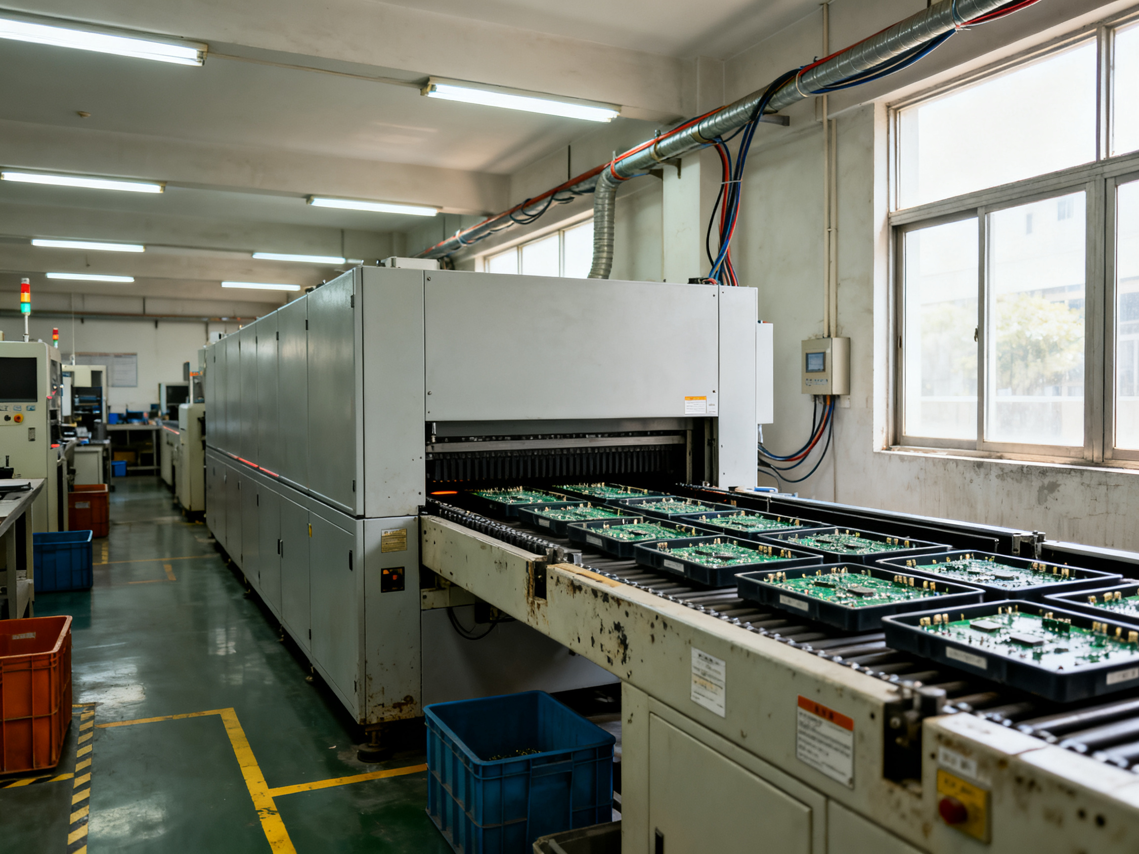
This guide walks through both processes end to end: how reflow soldering works, temperature profiles and real limits, the reflow oven and wave soldering machine hardware, SMT line setup, solder paste and flux selection, common BGA and QFN defects, validation and records, operating costs, and a straight framework for choosing equipment. The standards referenced throughout, including IPC J-STD-001J and IPC-A-610J, matter because they set the acceptance bar your customers will hold you to.
Author bio: [Author Name] is [verified title or credential] with experience in [verified area relevant to SMT equipment, reflow soldering, wave soldering, or electronics manufacturing]. [He/She/They] has contributed to [verified project, role, achievement, certification, or manufacturing responsibility]. Replace all placeholders only with supplied and fact-checked information.## About the Author
[Author Name] is [verified role or credential] with experience in [verified area of SMT, electronics manufacturing, or soldering expertise], including hands-on responsibility for [verified area of responsibility: reflow ovens, wave soldering, process engineering, or SMT production lines].
They also hold [verified achievement, project, certification, or manufacturing responsibility], which will be listed here once confirmed.
This section is a placeholder pending publication of verified details. A professional headshot and a link to a full author profile will be added at the same time, so nothing appears that has not been fact-checked against internal records.## 1. What Is Reflow Soldering, and How Does It Work?
So what does reflow mean in soldering? Short answer: the solder does not melt on your workbench, it melts on the board itself. A reflow soldering oven heats the entire populated assembly until the solder paste sitting on each pad melts, wets the component terminal and pad, then cools into a solid metallurgical joint. Every surface-mount joint on that board forms inside one controlled thermal cycle. That single fact is why reflow dominates modern PCB production.
Think of what a reflow soldering machine is doing in simple terms. It is a conveyor oven with a series of independently controlled heating and cooling zones. The board rides a conveyor from cold to hot to hot again to cold, while each zone holds its own setpoint. Hot air moves across the board, so the thermal profile can be shaped to match the paste and the packages on it.
Here is the standard reflow soldering process, step by step:
- Stencil printing. Solder paste is squeegeed through a laser-cut stainless stencil so each land gets a controlled deposit.
- Solder paste inspection. SPI checks deposit volume, area, height, and alignment before anything is placed.
- Component placement. Pick-and-place heads set components into the paste. The paste holds them, so no glue or clamp is needed.
- Profiling setup. Thermocouples are attached to the board’s hot and cold locations, usually on a sacrificial sample.
- Preheat and ramp. The board comes up to temperature gradually so components do not thermal shock.
- Soak. A dwell zone lets flux activate and the board equalize.
- Reflow. The oven crosses the alloy’s liquidus, roughly 217 C for common SAC alloys, and holds above it long enough for wetting to finish.
- Cooling. Controlled cooling sets the joint microstructure and fixes solder-ball formation risk.
- Inspection. AOI for visible joints, X-ray or CT for hidden BGA and QFN joints.
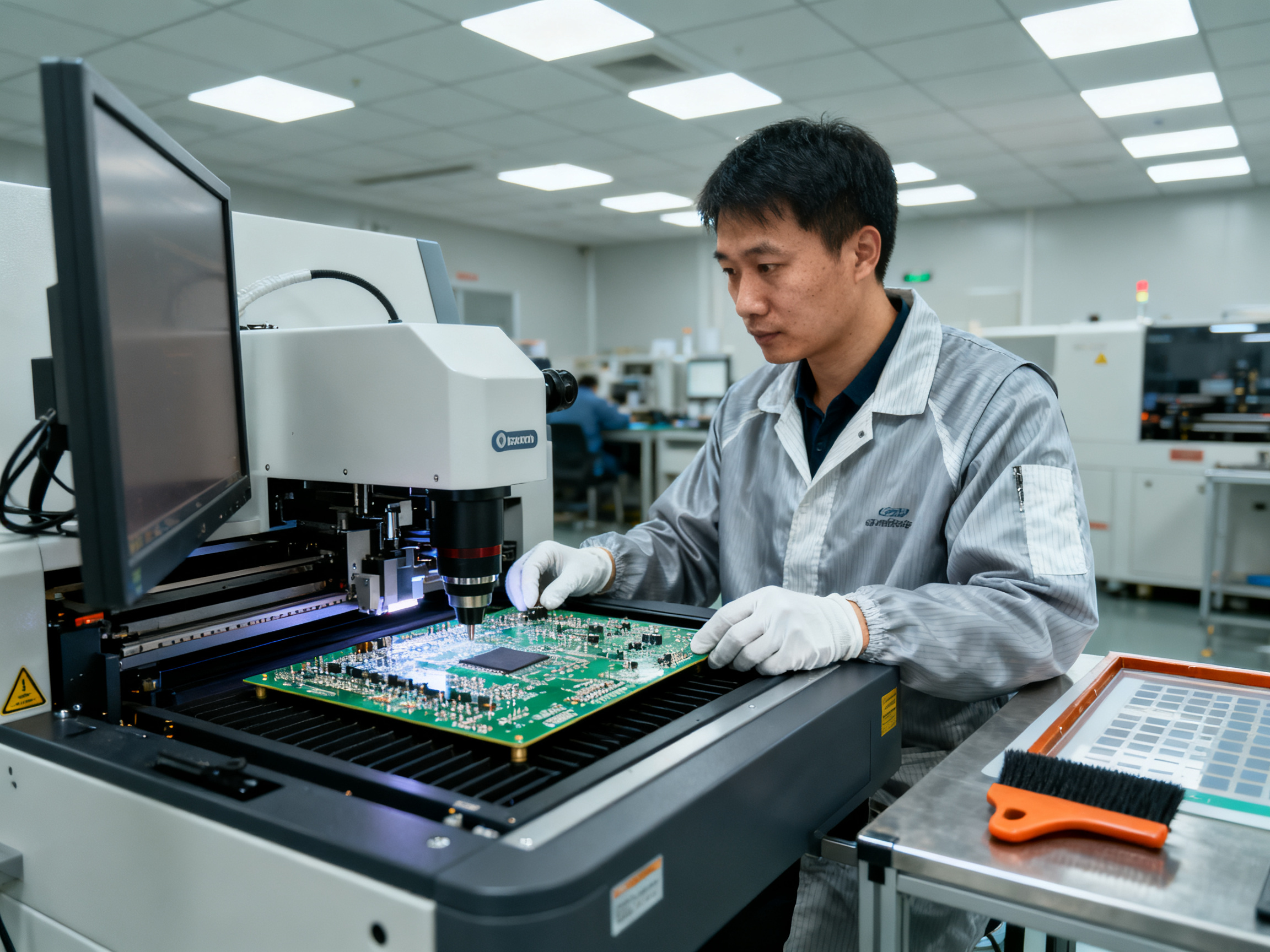
That sequence, paste printing through inspection, is the backbone of nearly every SMT line in production today, and equipment makers such as S&M Co. Ltd. (Shenzhen Chuxin Electronic Equipment Co., Ltd.) build lead-free reflow ovens and full SMT lines around exactly this flow.
Expert Tip: The center-zone setpoint alone does not prove that every solder joint experienced an acceptable thermal profile. An oven can sit perfectly on its recipe and still cook a small QFN or thermally soak a large BGA, so treat setpoints as the starting point and the measured board profile as the only real evidence. Supplier documentation such as Indium’s reflow profiling technical paper gives the SAC windows worth starting from, and IPC-A-610J sets the acceptance bar for what a finished joint should look like.
One more piece of the hardware puzzle. Beyond heating and cooling zones, a modern reflow oven needs exhaust and condensate management, filtered laminar airflow across the board, nitrogen option for oxidation control, data logging per board, and traceability hooks into the line. Those details decide whether two shifts in a row produce the same result, which is the only test that matters when you are shipping to a customer.## 2. What Is Wave Soldering, and How Does It Work?
Where reflow heats the whole board from above, wave soldering does something much simpler and more physical: it drags the underside of the board through a controlled wave of molten solder. The leads of through-hole components push up into that wave, the solder wets the lead and the plated barrel of the hole, and as the board lifts away the solder pulls back, leaving a filled joint. That is the whole idea.
Here is the wave soldering process, in order:
- Board preparation. The PCB is loaded, often into a custom pallet or mask when bottom-side parts need protection.
- Flux application. A spray or foam fluxer coats the underside and wets the holes.
- Preheat. Top and bottom preheat zones bring the board toward an activation temperature so the flux does its work without boiling it off.
- Wave contact. The board meets the solder wave, either a turbulent chip wave or a smoother laminar wave.
- Controlled withdrawal. The board exits at a set angle and speed so solder drains instead of pulling into icicles.
- Cooling. Air or chiller-assisted cooling fixes the joint.
- Cleaning. Water-soluble flux lines get washed; no-clean lines usually do not.
- Inspection. Visual plus AOI for the surface, X-ray or cross-section when internal barrel fill is in question.
WAVE SOLDERING MACHINE: MODULE LAYOUT (board travel left to right)
 +-----------+  +-----------+  +-------------+  +------------------+
 | Conveyor  |->| Fluxer    |->| Preheater   |->| Solder Pot +    |
 | + Pallet  |  | spray/foam|  | top/bottom  |  | Wave (chip or   |
 |   Loader  |  |           |  | tunnels     |  | laminar) +      |
 +-----------+  +-----------+  +-------------+  | Nitrogen Hood   |
                                                 +------------------+
                                                          |
                    +----------------+                   v
                    | Cooling Fan /  |------------->| Fume Extraction|
                    | Chiller        |                | + Dross Filter |
                    +----------------+                +----------------+
SIDE VIEW: PCB CONTACT WITH THE SOLDER WAVE
        board top
  ============================  ------
      |    |    |   |    |          lead / plated barrel
      \____/    |   |    |          solder wets lead + hole wall
  ---------------------------------  PCB bottom
      ~~~~~~~ ~~~~~ ~~~~~ ~~~~~   <-- molten solder wave (laminar crest)
   ~~~~~~~~~~~~~~~~~~~~~~~~~~~~~ <-- solder pot bath
   ~~~~~~~~~~~~~>                <-- travel direction; board tilts on exit
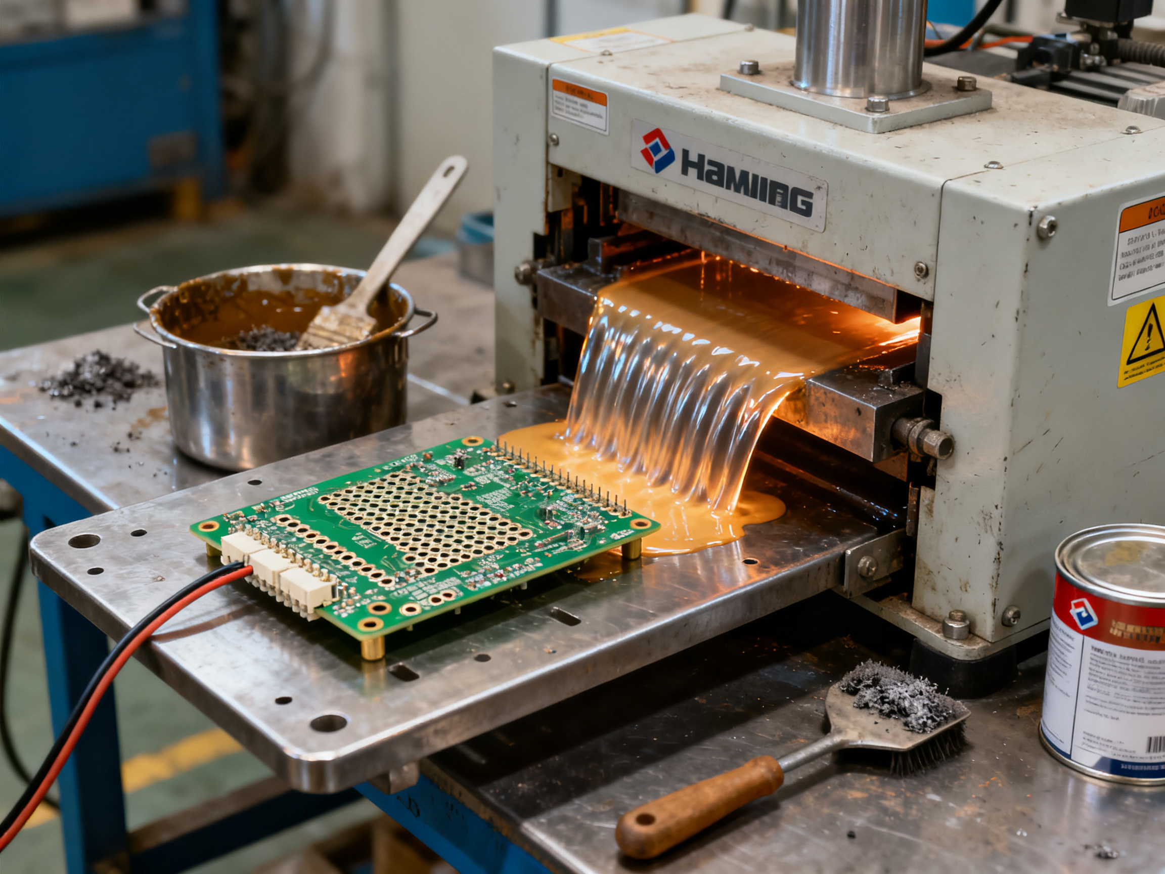
The dual-wave setup is worth understanding. The first wave is turbulent, which pushes solder into dense holes and helps wet stubborn geometries. The second wave is laminar, and it exists to drain cleanly and cut bridging. Fine pitch bottom-side SMD, tall parts, limited edge clearance, and thick boards with big copper planes all narrow the process window. When a full wave cannot reach a joint without cooking its neighbour, selective soldering is usually the better answer.
Every number on a wave machine is specific to the alloy, flux, board, and pallet combination. Product-specific windows exist, such as the lead-free pot and preheat ranges listed in Indium’s WF-9958 wave solder flux data sheet, and alloy-specific contact guidance in the Indalloy 291 technical note. Profiling and process control follow the framework in IPC-7530B, and IPC-AJ-820A covers the acceptability side of the process.
Wave soldering still earns its keep in 2026 on stable, high-volume through-hole product. Equipment makers such as S&M Co. Ltd. (Shenzhen Chuxin Electronic Equipment Co., Ltd.) build wave soldering machines alongside lead-free reflow ovens and complete SMT lines for exactly that kind of work.
One practical note before you spec a machine. It is tempting to compare a wave machine’s price to a reflow oven’s price and call it a budget decision. It is not. The real cost lands in pallets, nozzles, flux, bar solder, dross removal, and the inspection you need to catch fill defects that nobody can see on the board surface.## 3. Reflow Soldering vs. Wave Soldering: Key Differences
Here is the honest version of the comparison. Reflow and wave are not competing answers to the same question. They solve different geometry problems, and most mature lines run both.
Reflow wins on density. Fine-pitch SMD, BGAs, QFNs, and anything with a high pin count across a board need a process where every joint forms simultaneously under one profile. Wave wins on volume of simple through-hole work, where the geometry is stable, the leads are forgiving, and the pot is cheaper to run than the oven.
| Factor | Reflow Soldering | Wave Soldering |
|—|—|—|
| Application | Dense SMT, mixed-technology boards | High-volume through-hole, connectors, panels |
| Component types | BGA, QFN, fine-pitch SMD, 01005 | THT leads, headers, connectors, shielding |
| Heating method | Forced hot air over the whole board | Board underside dragged through a molten wave |
| Temperature control | Per-zone setpoints plus measured board profile | Pot temperature, preheat zones, contact time, withdrawal angle |
| Throughput | High, continuous conveyor | High, but slower for small boards without pallets |
| Changeover | Recipe-driven, fast | Pallet and tooling changes add real time |
| Consumables | Paste, stencils, solder balls in stencils | Bar solder, flux, pallets, nozzles, dross skim |
| Typical defects | Head-in-pillow, voids, bridging, insufficient wetting | Insufficient fill, icicles, bridging, solder balls, skips |
| Capital cost | Higher | Lower |
| Operating cost | Lower per joint at volume | Higher per joint once pallets and dross are counted |
| Nitrogen use | Common for appearance and dross control | Optional hood for pot oxidation |
| Inspection | AOI plus X-ray or CT for hidden joints | Visual, AOI, X-ray for barrel fill |
| Ideal use case | Smartphone, semiconductor, dense and mixed boards | Stable THT product, repeat builds, controlled geometry |
Anonymized example. A medical device maker came to us with a 40-part mix of through-hole connectors and a handful of fine-pitch SMD parts. They ran everything through a wave machine and were rejecting roughly 3 percent of boards for bridging near a tall relay. We split the work: reflow handled the fine-pitch top side, and a wave machine with a custom pallet took the through-hole bottom. Scrap dropped to under 0.5 percent. The extra capital paid for itself inside a year, which is not always the case, so measure your own boards before you trust that kind of number.
PROCESS SELECTION FLOWCHART
        Start
          |
  Does the board have BGA, QFN,
  or fine-pitch SMD?
     /            \
   YES             NO
    |               |
 Reflow         Is most work through-hole
 (plus wave or    with stable geometry and
 selective for     high volume?
 bottom side)      /          \
                YES            NO
                 |              |
             Wave solder     Consider reflow
             with pallet     for mixed boards, or
                            selective soldering for
                            high mix, localized joints
And the third option deserves a real mention. Many lines do not pick one. They combine reflow for the top side with wave for the bottom, then add selective soldering for the handful of joints a full wave cannot reach without cooking a neighbour. That third leg is what keeps high-reliability work in one facility instead of shipping boards to a job shop.
Standards treat these as separate controlled processes, which is why you will see wave soldering guidance documented apart from the reflow rules, including the process windows outlined in IPC’s wave soldering technical resource.
Pro Insight: Reflow and wave are usually the wrong thing to compare. Compare your worst board and your best board against each process, and the answer usually writes itself. Then budget for the third process, selective soldering, because mixed assemblies rarely fit one clean answer.## 4. Reflow Soldering Temperature Profile: Zones, Targets, and Limits
Every reflow soldering temperature profile has the same shape. It ramps up gently, holds, spikes, then falls. The curve looks simple. Getting a board through it correctly is the hard part.
The profile has five stages, and each one has a job.
LEAD-FREE SAC PROFILE SHAPE (illustrative, board temperature vs time)
  deg C
   260 |                    ****
       |                   *   *        <- PEAK: 230-260 C
   217 |-------------------*-----*------- <- LIQUIDUS: ~217 C (SAC)
       |          [ SOAK ] *       *       140-170 C, 30-120 s
       |        /                *
       |      /                   *  \   <- COOLING: 0.5-6 C/s
   150 |    /                      \
       |  /                         \
    25 |/____________________________\____  <- RAMP: 0.5-2.5 C/s
       +--------------------------------------------> time
          preheat      soak      TAL    cool
Preheat and ramp bring the board up from ambient at a controlled rate. Too fast and you thermal shock big packages. Too slow and flux burns off before it can do its job.
Thermal soak is a dwell at a moderate temperature, usually 140 C to 170 C for SAC alloys. It lets the whole board reach the same temperature, which shrinks the spread between your hottest and coldest joints.
Time above liquidus is the wetting window. For SAC305 and similar alloys, liquidus sits near 217 C, so the joint stays molten long enough for the solder to spread properly.
Peak temperature is the highest point on the curve. It must be high enough for good wetting, and low enough to spare the package, the laminate, and any temperature-sensitive part.
Cooling fixes the joint structure. Rushing it can trap voids and weaken large thermal joints.
PROFILE STAGE GUIDE (indicative SAC starting points, not universal settings)
 Stage        | Purpose                    | Indicative range | Too low                          | Too high
 -------------|----------------------------|------------------|----------------------------------|--------------------------------
 Ramp         | Even heat, no shock        | 0.5-2.5 C/s      | Cold joints, oxidation            | Thermal shock, lifted pads
 Soak         | Equalize board temp        | 140-170 C,       | Wide delta-T, dry joints          | Flux burns off, graping
              |                            | 30-120 s         |                                  |
 Above        | Wetting and joint flow     | 30-100 s         | Poor wetting, opens               | Intermetallics, voiding
 liquidus     |                            |                  |                                  |
 Peak         | Full melt                  | 230-260 C        | Cold solder balls                 | Package or laminate damage
 Cooling      | Solidify cleanly            | 0.5-6 C/s        | Slow, uneven grain               | Voids, cracked joints
Pro Insight: Profile the hardest-to-heat and most temperature-sensitive locations, not one convenient spot. A thermocouple on a mid-size resistor tells you very little about a large BGA or a fragile connector. Attach beads to the BGA center and edge, the QFN thermal pad, a large copper plane, and your lowest-rated part. Then read the trace, not the oven recipe.
Here is where experience helps more than theory. A board profile looked fine on paper, yet one row kept pulling components off center. The culprit was not the oven. It was ramp speed. Dropping the ramp from about 1.8 C/s to 1.0 C/s and extending soak by 20 seconds evened out the delta-T and the shifting stopped.
Supplier documents such as Indium’s reflow profiling technical paper give the SAC windows worth starting from, and paste data sheets like Kester 70-4823 list the profile each specific paste needs.
One safety note, and it is not optional. These numbers are starting references. Your actual settings depend on the alloy, the paste spec, component maximum ratings, board mass, and oven capability. Validate on your own product before you commit to a recipe in production.
Tin-lead (Sn63/Pb37) behaves differently. Liquidus is around 183 C and peak temperatures run lower, but do not borrow a SnPb profile for a SAC board without measuring it. Lead-free conversion changes thermal load, wetting behavior, voiding, and fatigue all at once, so treat it as a new process, not a swap.
Measure what happens twice. Run the same profile on three boards, compare the traces, and only then call the recipe stable. And check delta-T on the worst board in the family, since that one decides your yield.## 5. Wave Soldering Temperatures and Critical Setup Parameters
Wave soldering is the one process on the SMT line where temperature becomes a physical event rather than a curve on a screen. The pot holds molten solder. The board meets it, and for a few seconds the alloy either flows into the hole or it does not. Everything else on the machine exists to make those seconds predictable.
The first thing to unlearn is the idea that pot temperature equals board temperature. It does not. The board arrives at the wave already heated by the preheat zones, so the pot adds the final melting step. Run a board cold into a hot pot and the joints fill but the flux never activates. Run it too hot and you cook the laminate, dissolve copper, and warp the panel. That is why flux activation and topside preheat are tied to the pot setting rather than independent of it.
Lead-free and tin-lead are different animals. Lead-free pots typically run hotter, need longer dwell to wet properly, and demand more attention to dross control. Tin-lead runs cooler and shorter but still needs its own window. Numeric values must come from your alloy supplier, flux data sheet, board finish, and component ratings, because a copper-heavy board drinks heat like a sponge and a thin lead-free board heats almost instantly.
CONTACT TIME AND BOARD ANGLE: THE WITHDRAWAL WINDOW
     board travels left to right, exit angle 4-8 deg
        /  rising exit angle
       /_______________________________
      |    |    |    |    |    |         <- leads in plated barrels
   ~~~|~~~~|~~~~|~~~~|~~~~|~~~~|~~~~     <- solder crest
   ~~~~~~~~~~~~~~~~~~~~~~~~~~~~~~~      <- pot bath
             |<- contact time ->|       <- 3-5 s (SnPb 1.5-3 s typical)
   immersion depth ~ 1/2 to 2/3 of board thickness
Too steep an exit angle and solder drags out of the hole, leaving icicles. Too shallow and you get poor drainage and bridging. And if the conveyor speed does not match the effective wave length on your machine, the contact time changes completely, which is why conveyor speed numbers are not transferable between machines. Specify measured contact time first, then record the speed that produces it.
Dwell, immersion, and wave height all pull on each other. Longer dwell fills stubborn holes but bridges dense leads. More immersion improves wetting and increases bridging at the same time. A turbulent wave pushes solder into tight geometry and also spits solder balls onto the board.
Here is the setup map we work from:
| Parameter | How to measure | Typical starting range | Interacts with | Likely defect if wrong |
|—|—|—|—|—|
| Solder pot temperature | Pot thermocouple, daily check | Lead-free 265-270 C, SnPb 245-260 C | Preheat, alloy, flux solids | Poor fill, dross, copper dissolution |
| Topside preheat | Board thermocouple or IR | 85-120 C | Bottom preheat, board mass | Flux burns off, dry joints, warpage |
| Bottom preheat | Board thermocouple | 85-125 C | Topside preheat, board mass | Skips, nonwetting, bubbling |
| Contact time (dwell) | Timed pass, oscilloscope or video | 3-5 s lead-free, 1.5-3 s SnPb | Conveyor speed, wave length, pot temp | Insufficient fill, bridging |
| Conveyor speed | Machine readout, verify in seconds | 0.9-1.8 m/min band | Wave length, contact time | Fill inconsistency, skipping |
| Wave height | Rule or sensor, across path | 1.5-2.5 mm above pot lip | Pump speed, immersion | Solder balls, bridging, icicles |
| Board angle | Fixture measurement | 4-8 deg exit tilt | Withdrawal speed, pallet design | Icicles, trapped solder |
| Immersion depth | Fixture measurement | 1/2 to 2/3 board thickness | Wave height, board thickness | Over-immersion bridging, warpage |
| Cooling | IR or contact thermography | Controlled ramp after exit | Flux residue, warpage | Solder balls, stress on joints |
Dwell guidance like this comes from the flux and alloy suppliers themselves; Kester’s NF1060-VF technical data sheet lists typical dwell of 3 to 5 seconds for Sn63/Pb37 and 4 to 8 seconds for lead-free alloys, and the machine, board, and pallet combination still has the final word.
Get these five setup checks right before you touch the recipe: pump and nozzle stability, wave shape and height across the actual path, board flatness in the pallet, measured flux solids and coverage, and scheduled bath analysis for alloy composition and copper trend. That last one catches copper dissolution before it becomes a warpage problem.
The pattern of failure is consistent. Insufficient fill points to low local temperature, weak flux, short contact, or heavy copper heat sinking. Bridges and icicles point to over-immersion, poor drainage, or long dwell. Skips point to flux, contamination, or shadowing. Solder balls point to excess flux, spatter, or turbulence. And warpage, copper loss, and component damage all point back to too much heat for too long.
One more practical note. Schedule dross removal and bath analysis like you schedule calibration. Dross reduces effective wave height, and a slow drop in wave height looks a lot like a temperature problem until you look at the pot.
Next, we get into the hardware itself, the reflow soldering oven and the wave soldering machine, and what to specify when you are actually shopping for one.## 6. Reflow Oven and Wave Soldering Machine Setup for an SMT Production Line
Buying the oven is the easy part. The install is where schedules slip, and a slipped install eats margin faster than any bad purchase.
Here is the pre-installation checklist we work from before anything is delivered:
| Item | Reflow Oven | Wave Machine | Why it matters |
|—|—|—|—|
| Electrical service | Nameplate kW, phase, inrush, SCCR | Same, plus pot heater duty | Under-sizing the feed causes nuisance trips at startup |
| Compressed air | For cooling assist and shutters | For fluxer and cooling | Confirm pressure and dryer on the line |
| Nitrogen | Purity, regulator, flow metering | Hood supply if used | Nitrogen needs an oxygen-deficiency risk assessment and monitoring |
| Exhaust | Flow rate, static pressure, condensate | Larger volume, rosin and metal fume | Size the duct to the machine, not the room |
| Floor and point loads | Floor flatness, machine mass | Plus pot mass with full pot of solder | Check point loading under the pot |
| Service clearance | Door swing, filter and fan access | Pallet change, dross skim, pot service | Plan the route for a 25 kg solder pot |
| Conveyor height and direction | Match upstream printer and AOI | Match loader and washer | Height mismatch causes transfers to be hand-worked |
| Board dimensions | Max board, max weight, panel support | Pallet and mask tooling | Defines your usable window |
| Network and MES | Ethernet, traceability, barcode | Barcode and MES link | Decide who owns recipe and history data |
| Safety | E-stops, exhaust and fan interlocks, over-temp cutout | Plus solder-level protection, burn guards | Reviewed with your AHJ, not assumed |
SMT LINE LAYOUT (left to right, load to ship)
 [Loader] -> [Printer] -> [SPI] -> [Pick&Place] -> [Reflow Oven] -> [AOI] -> [X-ray] -> [Unloader]
                   |                                                          |
                   +-- stencil wash/clean station                            |
                        [Loader] -> [Selective/Wave Solder] -> [Cooling] -> [Wash] -> [AOI]
                        Above: MES server, barcode scan, humidity control,
                        exhaust tie-in, nitrogen manifold, compressed air
Line communication is worth getting right on day one. IPC-HERMES-9852 handles board transfer and identity, and IPC-2591 CFX carries process data both ways to your host system. Ask the vendor to demonstrate a reject, a jam, a duplicate barcode, and a network drop during the acceptance test. A machine that only works on a clean golden path is not integrated.
Recipe creation and changeover
Each board family gets a recipe, and the recipe is a controlled document. For reflow, that means board support type, conveyor speed, per-zone setpoints, cooling fan output, and alarm limits. For wave, it adds flux solids, preheat targets, wave height, conveyor speed, and pot temperature. Every recipe change runs a first article, and first article gets signed before the run continues.
Procurement scorecard
Score each vendor 1 to 5, then weight by what matters to you:
| Criterion | Weight for SMT volume | Weight for high mix |
|—|—|—|
| Usable process window (measured, not brochure) | High | High |
| Thermal uniformity and delta-T under load | High | Medium |
| Profile repeatability across 10 runs | High | High |
| Maintenance access and spare parts lead time | High | High |
| Remote diagnostics and software lifecycle | Medium | High |
| Energy and nitrogen consumption per board | High | Low |
| Data logging, traceability, MES integration | High | High |
| Local service response and restoration times | High | High |
| Compatibility with your printer, SPI, AOI, X-ray | High | High |
| Capital cost and total cost of ownership | Medium | Medium |
The last row is where vendors go quiet. Ask for good boards per hour including warm-up, cleaning, changeover, and recovery, not just cycle time. Ask for installed-base references with comparable boards, not similar industries.
Expert Tip: Accept the machine on your worst-case board with your actual paste, not on a sample board the vendor brought with it. That one trial will tell you more than every brochure in the packet.
Equipment like the lead-free reflow ovens, wave soldering machines, and complete SMT lines built by S&M Co. Ltd. (Shenzhen Chuxin Electronic Equipment Co., Ltd.) is typical of the category, so ask any vendor the same hard questions about process window, repeatability, and lifecycle support before you sign.
Next: Section 7 covers solder paste printing and flux selection, the material choices that quietly decide whether your profile even works.## 7. Solder Paste, Flux, Nitrogen, and Material Selection
Materials quietly decide whether your profile even works. A perfect thermal curve cannot rescue the wrong paste on the wrong aperture.
Solder paste is not one product. It is an alloy (SAC305, SAC305 with additions, or Sn63/Pb37 for legacy work), a powder size distribution (Type 1 to Type 5 or beyond), and a flux chemistry graded under IPC J-STD-004D. Each variable changes the result. Finer powder fills small apertures better but oxidizes faster and demands tighter handling. Higher viscosity holds shape on the stencil, lower viscosity prints easier but slumps more during idle time.
Warning: Do not choose a paste by melting point alone. Two pastes with the same alloy and liquidus can behave completely differently on the line, because viscosity, thixotropic recovery, slump, tack life, stencil life, and flux activity decide whether the deposit prints right and stays right until the oven reaches it. Always qualify against your own apertures and your own profile, and read the Indium 8.9HF1 no-clean paste data sheet style specification sheet for the specific product, not for the alloy family.
| Selection factor | What to check | Why it changes the outcome |
|—|—|—|
| Alloy | SAC grade, silver content, liquidus | Sets peak temperature, wetting, fatigue life |
| Powder size | Type 1 to Type 5 | Aperture fill, oxide surface area, handling |
| Flux classification | J-STD-004 class, activity level | Activating ability, residue, corrosion risk |
| Viscosity | Method and temperature stated | Print consistency across the shift |
| Slump and tack | Room and hot slump, tack life | Placement hold, deposit stability after idle |
| Stencil life | Print cycles and shelf time | Drag-out, bridging, solder balls |
| Storage and thawing | Seal, warm-up time, humidity | Condensation, viscosity drift, oxidation |
Wave soldering needs its own flux logic. Activity level, solids content, coverage uniformity, residue and cleaning compatibility with your board finish all matter, and application consistency (spray versus foam) changes the deposit you actually get on the barrel.
And then there is nitrogen reflow soldering. Nitrogen can cut oxidation, improve wetting, reduce dross, and clean up appearance. But nitrogen is not a void cure, and it is not automatic insurance. It costs gas, plumbing, monitoring, and an oxygen-deficiency risk review. Justify it on measured benefit for your product, not on vendor folklore.
Storage rules are boring and profitable. Keep containers sealed while they warm to room temperature, avoid air entrainment when mixing, and never return used paste to fresh stock unless the supplier explicitly allows it.
Next: Section 8 covers common defects in BGA, QFN, SMD, and through-hole soldering, plus how to find the real root cause instead of blaming the oven.## 8. Common Defects in BGA, QFN, SMD, and Through-Hole Soldering
Almost every soldering complaint gets blamed on the oven. Sometimes the oven is guilty. Often it is not.
The trick is to stop guessing and start mapping. Reflow defects cluster around printing, placement, thermal profile, material, and design causes. Wave defects cluster around flux, preheat, wave shape, conveyor setup, and board geometry. A short matrix gets you there fast.
| Symptom | Likely causes | Verify with | Corrective action |
|—|—|—|—|
| Bridging (fine pitch) | Too much paste volume, wrong aperture, slump after idle, board shift | SPI deposit volume and area, cross-section | Reduce deposit volume, clean apertures, control idle time |
| Head-in-pillow / non-wet opens | Package or board warpage, weak flux, poor profile, pad design | 3D X-ray, dye-and-pry, cross-section | Improve flatness, soak for equalization, verify flux activity |
| Voiding in BGA/QFN | Trapped volatiles, large deposit, limited escape path, via wicking | 2D X-ray screening, CT for depth, cross-section | Small deposits, longer soak, dedicated escape vias |
| Tombstoning | Uneven heating, ramp too fast, small unsupported parts | AOI, cross-section | Slow the ramp, extend soak, check pad symmetry |
| Solder balls | Flux spatter, slump, poor reflow, dirty stencil | AOI, process log | Filter and age the paste, clean stencil, check filter life |
| Component shift | Placement offset, paste slump, board movement, thermal imbalance | SPI, AOI, placement data | Fix placement, improve paste stability, control conveyor drift |
| Insufficient THT fill | Low local temperature, short contact, weak flux, copper heat sinking | X-ray or cross-section of barrel | Raise preheat and pot temp, lengthen dwell, improve flux |
| Icicles | Too-steep exit angle, poor drainage, over-immersion | Visual | Set 4-8 deg exit, reduce immersion, check withdrawal speed |
| Skips / blowholes | Flux depletion, contamination, shadowing, venting blocked | Visual, X-ray | Check flux solids, clean board, open up vent holes |
Void percentages get argued about constantly. NASA’s published work on QFN voiding is worth reading here, because it shows why there is no single universal limit: interpretation depends on joint geometry, thermal path, edge location, and service load. The same logic applies to BGA thermal joints.
Now the sequence. This is the part most lines skip, and skipping it is why the same defect keeps coming back.
- Confirm the defect. Electrical test shows an open, not a cause. X-ray, dye-and-pry, or cross-section tells you what actually failed.
- Segment it. Sort by board, component, lot, machine, and shift time. A defect that tracks one lot of paste is a material problem, not an oven problem.
- Verify your measurement system. Check inspector agreement, AOI algorithm false calls, and thermocouple attachment repeatability before trusting the data.
- Inspect upstream. Print, SPI, placement, and material handling come before the oven in the causal chain.
- Review profile and machine data. Pull the actual board trace, not the recipe. Pull pot temperature, dwell, flux solids, and wave height for wave work.
- Change one variable. One controlled change, one measurable outcome.
- Document it. Record the defect, cause, change, and result so the next shift inherits the answer.
One case from a line we support: recurring “cold” through-hole joints on a control board turned out not to be a temperature issue at all. X-ray showed acceptable fill, and the pot was holding spec. The real cause was a flux drum swapped for a lower-solids batch, leaving the barrel walls poorly activated. Temperature held, the joint simply never wetted. Nobody in the fab had checked flux solids since commissioning.
Acceptance criteria for the repaired joint come from IPC-A-610J and IPC J-STD-001J, and void interpretation guidance is well covered in NASA’s QFN voiding analysis. Keep both close, because “the board looks fine” is not a standard.
Next: Section 9 covers soldering process validation and the records you need to keep.## 9. How to Validate and Control the Soldering Process
Validation is not paperwork. It is evidence that your chosen reflow oven or wave soldering machine, your materials, your recipe, and your inspection plan consistently produce assemblies that meet documented requirements, at the volume you actually run.
Here is the order that works.
- Requirements and risk review. Define the product class, applicable standards, and the risks that matter. Automotive work pulls in IATF 16949 and the automotive addendum; space and aerospace work pulls in AS9100 and NASA workmanship documents, such as NASA-STD-8739. Commercial work runs on IPC J-STD-001J with IPC-A-610J.
- Measurement system confirmation. Before any number means anything, check inspector agreement, AOI false calls, and thermocouple attachment repeatability.
- Characterization and DOE. Prove the process window for your worst-case board and your most sensitive component, not the sample board.
- Capability analysis. Only after the process is stable and the measurement system is trustworthy.
- First article build. Production-intent materials, real operators, signed results.
- Reliability testing tied to the actual mission profile.
- Control plan and change control. This is where validation becomes daily work.
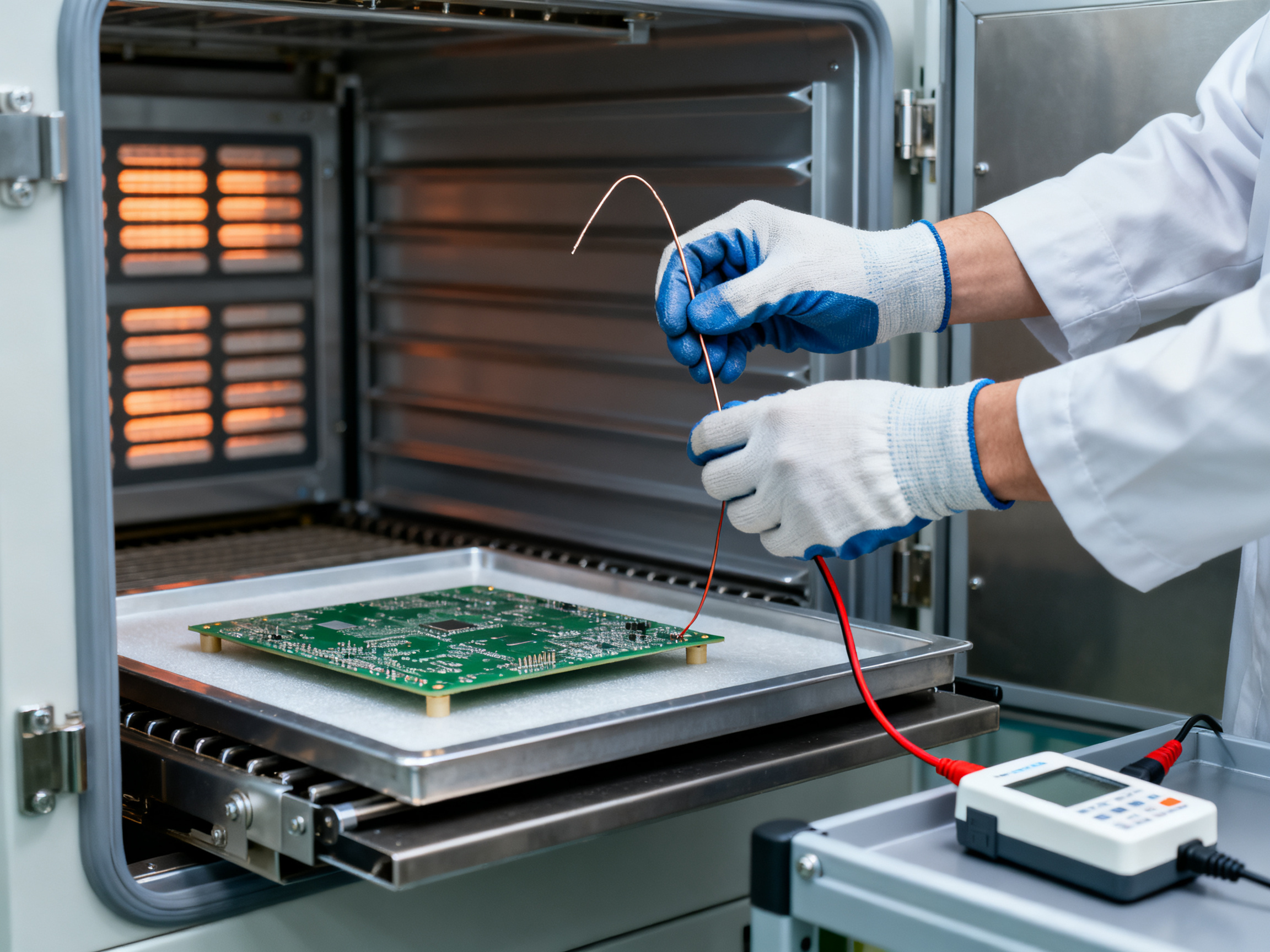
VALIDATION WORKFLOW
 Requirements & risk review
          |
 Measurement system analysis (MSA)
          |
 Profile / parameter characterization (+ DOE)
          |
 Capability analysis on stable process
          |
 First article build (production intent)
          |
 Reliability test (mission profile)
          |
 Control plan + SPC limits
          |
 Ongoing monitoring --> change control --> requalify
The control plan is short, and every line needs an owner, a frequency, and a reaction rule.
| Characteristic | Method | Frequency | Reaction if out of limit |
|—|—|—|—|
| Board profile vs. recipe | Thermocouple profile | Per lot / after change | Quarantine lot, re-profile |
| Paste deposit volume | SPI | Every board | Stop line, check stencil |
| Pot temp and wave height | Gauge check | Daily, each shift | Adjust, re-check fill |
| Flux solids | Titration | Daily | Add flux, re-verify |
| Solder bath composition | Lab analysis | Scheduled | Top up, skim dross |
| AOI / X-ray results | Automated | Every board | Quarantine, root cause |
| First-pass yield | Line report | Daily / weekly | Pareto review |
Ongoing control ties back to the same list. SPC on first-pass yield, DPMO, rework rate, profile compliance, downtime, and solder consumption, plus a monthly defect Pareto across boards, lots, machines, and shifts.
SOLDERING PROCESS KPI DASHBOARD (line-level, weekly)
 First-pass yield ........ 97.4%  (target 97.0%)   [OK]
 DPMO ................... 4,900  (target <5,000)   [OK]
 Rework rate ............ 1.8%   (target <2.0%)   [OK]
 Profile compliance ..... 99.2%  (target 99.0%)   [WATCH]
 Unplanned downtime ..... 3.1%   (target <3.0%)   [WATCH]
 Solder consumption ... 2.4 g/board (baseline 2.5)[OK]
 Defect Pareto top 3: bridging 38% | voiding 27% | shift 19%
One statistical caution. A zero-defect sample does not prove zero defects. For independent trials the simple upper bound is p = 1 – alpha^(1/n), but clustered panel, reel, and machine effects need a different model. Do not quote a Cpk from a process that has not settled.
Retention matters as much as the numbers. Keep controlled recipes, material lots and certificates, profiles, AOI and X-ray results, calibration with as-found status, nonconformance dispositions, deviations, and every change with its requalification trigger. Retention periods follow your contracts, your quality system, and the product life risk.
Next: Section 10 covers soldering process cost, operating expenses, and how to build a realistic 5 to 10 year total cost of ownership.## 10. Which Process Should Your Factory Choose?
The honest answer is that most factories end up running more than one process, and that is a feature, not a failure. But the primary process still needs a clear owner.
Reflow soldering is the right anchor when your assemblies are dominated by high-density surface-mount parts and you need precise, repeatable thermal control. Wave soldering earns its place when high-volume through-hole work stays central and the board design supports full-wave access. Selective soldering fills the gap on mixed-technology boards where a full wave cannot reach a joint without cooking its neighbour.
Here is a weighted matrix. Adjust the weights to match your product mix rather than accepting ours.
| Criterion | Reflow | Wave | Selective |
|—|—|—|—|
| Fine-pitch, BGA, QFN capability | Strong | Weak | Moderate |
| Through-hole throughput | Weak | Strong | Moderate |
| Board geometry freedom | Strong | Limited by pallet and clearance | Strong |
| Process window predictability | High with thermocouple profiling | Medium | High |
| Changeover speed | Fast | Slower, tooling dependent | Fast |
| Capital and floor space | Higher | Lower | Medium |
| Cost per accepted joint at volume | Low | Medium | Medium |
Three illustrative scenarios, not case studies from our customer base:
Scenario A: dense consumer-electronics PCB. Fine-pitch, high component count, tight rework tolerance. Choose reflow as the backbone. Add X-ray inspection. Expect wave to be irrelevant here.
Scenario B: mixed automotive controller. Through-hole connectors plus a few fine-pitch parts on one board. Choose reflow for the top side and wave or selective for the bottom. Automotive addenda such as IPC J-STD-001JA and IPC-A-610JA also pull traceability requirements into the decision.
Scenario C: rugged military or aerospace assembly. Latent opens and contamination carry the real risk. Choose reflow with nitrogen control and strict documentation, plus selective soldering for localized joints. Expect the paperwork, not the machine, to be the long pole.
Before anyone signs a purchase order, get each function to answer its own question. Production asks about good boards per hour including warm-up and changeover. Engineering asks about the process window and the next product. Quality asks about invoked standards and acceptance criteria. Procurement asks about lifecycle cost, warranty, and obsolescence. EHS asks about extraction, nitrogen, and heat. IT asks about MES connectivity and data ownership.
One last thing. Run the trial on your worst board with your own paste. Vendors build machines for the best case; your line has to survive the other one. If you want a starting point for equipment that fits this profile, S&M Co. Ltd. (Shenzhen Chuxin Electronic Equipment Co., Ltd.) builds lead-free reflow ovens, wave soldering machines, and complete SMT lines for consumer electronics, semiconductor, and military work, and they are worth putting on your trial list.
Next: Section 11 covers the full cost picture, including a 5 to 10 year total cost of ownership model for reflow, wave, and selective soldering.## Conclusion: Build the Process Around the Assembly, Not the Machine
Reflow soldering and wave soldering are not competitors. They answer different assembly questions. Reflow forms every surface-mount joint at once under a profile you can measure, so it anchors dense, fine-pitch, and mixed-technology work. Wave soldering moves molten metal through plated barrels on stable, high-volume through-hole product. Selective soldering covers the joints a full wave cannot reach. The right answer depends on component technology, product requirements, process window, volume, and the whole manufacturing system, not the price tag of the machine.
Here is the seven-step checklist that holds up when a purchase order gets contested:
- Characterize the product. Worst-case board, densest assembly, lowest-rated part.
- Pull material specifications. Alloy, powder size, flux class, and the profile your paste requires.
- Profile or validate the process. Measure the board, not the recipe. The current standards set for the industry are listed in IPC’s recently released standards index, and they define the acceptance baseline.
- Compare total cost. Cost per accepted joint over 5 to 10 years, not purchase price.
- Run a representative trial. Your boards, your paste, your operators.
- Verify the data. Profile repeatability, traceability, and MES transactions witnessed at acceptance.
- Document acceptance criteria. Sign the limits before production starts.
Note to the editor: a first-person recommendation from the author has been withheld here because no author name, role, or credentials were supplied for this piece. It should be added only once a named author and documented experience are fact-checked.
Ready to move forward? Request a line assessment, a sample-board trial, a process consultation, or an equipment specification review from S&M Co. Ltd. (Shenzhen Chuxin Electronic Equipment Co., Ltd.), whose lead-free reflow ovens, wave soldering machines, and complete SMT lines are built for consumer electronics, semiconductor, and military production.
—## Planning Appendix: Research Priorities and Keyword Placement
Internal editorial note. Hold for desk review before publication.
Priority 1: Standards and process physics come first
Every temperature number, zone label, and acceptance threshold in this guide has to trace back to a primary technical source rather than a blog summary. That means the current IPC and JEDEC documents for ramp, soak, time above liquidus, peak, and cooling definitions, plus the exact paste and flux data sheet for any product we name. Check the published set against IPC’s index of recently released standards and documents before we lock the numbers, and treat supplier profile windows as starting points rather than limits.
Priority 2: 2026 figures, cost benchmarks, and defect examples
Market-size numbers in this piece come from commercial forecasting houses, not from a government or industry census. Label them as market research estimates every time, and never present them as production statistics. For defect examples, we want verified root causes with the evidence chain intact, since the line already works without that. For cost, build the 5 to 10 year model around accepted assemblies rather than purchase price, and run sensitivity cases for volume, yield, uptime, labor, utilities, and service.
Priority 3: Keyword placement
| Keyword | Planned placement |
|—|—|
| reflow soldering process | Title, Introduction, Section 1, image alt text, Conclusion |
| reflow soldering temperature | Section 4 and Section 5 |
| reflow oven, reflow soldering oven, soldering reflow oven | Section 6 and Section 10 |
| reflow soldering machine | Section 1 and Section 6 |
| what is reflow soldering, how reflow soldering works | Opening of Section 1 |
| smd soldering paste, best reflow solder paste | Section 7 |
| how to validate soldering process | Section 9 |
| wave soldering process | Section 2 and Section 3 |
| PCB soldering temperature profile, lead-free reflow profile | Section 4 |
| nitrogen reflow soldering | Section 7 |
| BGA and QFN soldering defects | Section 8 |
| soldering process validation | Section 9 |
Long-tail phrasing should read naturally rather than repeat mechanically. “What is reflow soldering in PCB” fits the Section 1 opening. “Temp to reflow solder” belongs in Section 4 where we explain the profile shape. “What is nitrogen reflow soldering” belongs in Section 7, and “how to validate soldering process” belongs in Section 9.
Suggested image alt text for the Section 1 hero graphic: Technician attaching a thermocouple to a PCB inside a reflow soldering oven during the reflow soldering process.
Sourcing discipline for the desk
Three things stay off the table until a named source supports them. There is no universal void percentage for BGA and QFN joints, no universal Cpk or sample size, and no blanket compliance claim for automotive, aerospace, or space work. Where void interpretation is discussed, point to the NASA QFN voiding work rather than inventing a threshold. And keep the author and reviewer fields as placeholders until real names, roles, and credentials are verified against internal records, along with any first-person callout that depends on documented experience.